Multi-chip packaging structure and manufacturing method thereof

A technology of multi-chip packaging and manufacturing methods, which is applied in semiconductor/solid-state device manufacturing, semiconductor/solid-state device components, semiconductor devices, etc., and can solve the difficulties in meeting the requirements of high performance, fast speed, multi-chip connection packaging and modularization, etc. problem, to achieve excellent heat dissipation effect, simple process structure, and short electrical path

Active Publication Date: 2021-06-25
FUDAN UNIV
View PDF3 Cites 0 Cited by
  • Summary
  • Abstract
  • Description
  • Claims
  • Application Information

AI Technical Summary

Problems solved by technology

The traditional wire bonding (semiconductor bonding gold wire) and double-sided copper clip interconnection process are difficult to meet these high performance, fast speed, multi-chip connection packaging and modular requirements

Method used


Image

  • Multi-chip packaging structure and manufacturing method thereof
  • Multi-chip packaging structure and manufacturing method thereof
  • Multi-chip packaging structure and manufacturing method thereof

Examples


Embodiment 1

[0042] In the embodiment, a novel chip packaging structure is provided, and the manufacturing method is as follows:

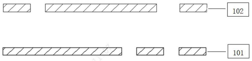
[0043] S101, provide patterned first metal substrate 101, second metal substrate 102 ( figure 1 ).

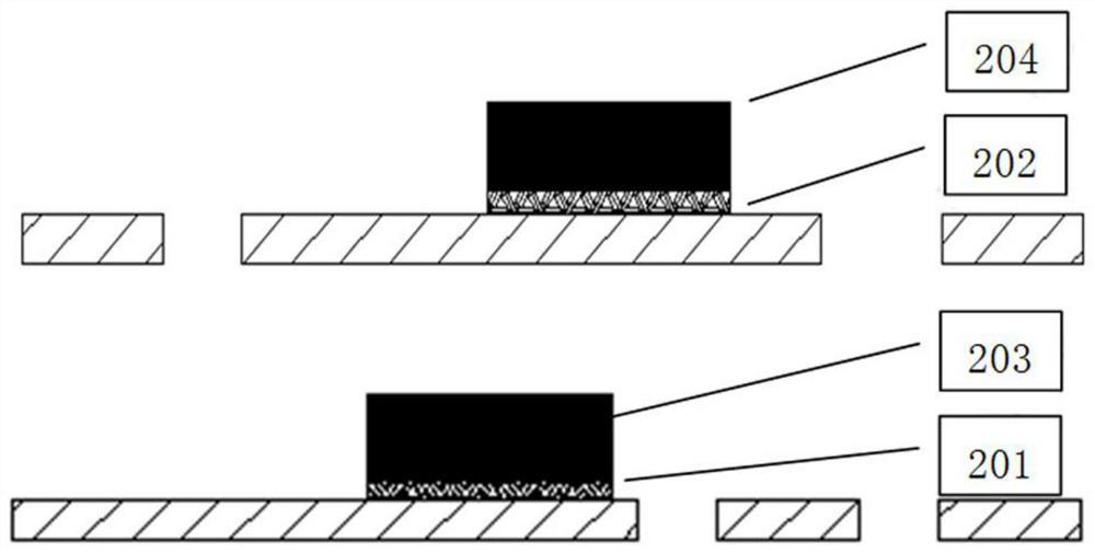
[0044] S102. Fabricate a first conductive layer 201 and a second conductive layer 202 on the first metal substrate 101 and the second metal substrate 102, and respectively place the first chip 203 and the first chip 203 on the first conductive layer 201 and the second conductive layer 202. Chip 204 ( figure 2 ).

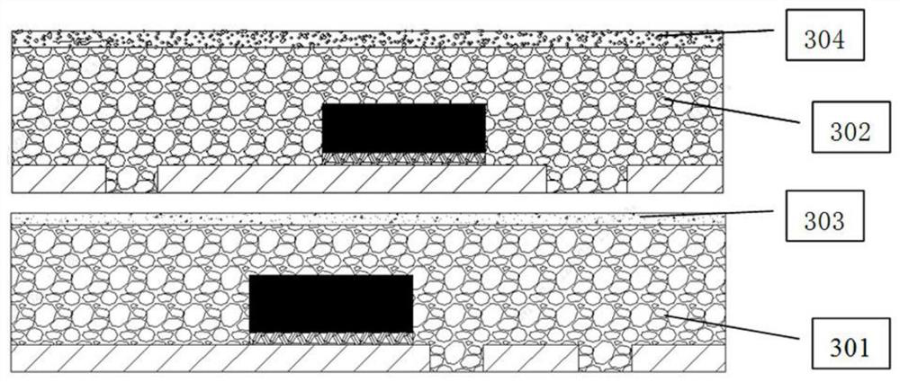
[0045] S103, on the first metal substrate 101, the second metal substrate 102, the side of the first conductive layer 201, the side sheet of the second conductive layer 202, the first chip 203, and the second chip 204, make the first dielectric layer 301 and the second dielectric layer layer 302 , on the first dielectric layer 301 and the second dielectric layer 302 , the seventh conductive layer 303 and the eighth conductive layer 304 are fabricat...


PUM


Abstract

The invention discloses a multi-chip packaging structure and a manufacturing method thereof. According to the multi-chip packaging structure and the manufacturing method thereof of the invention, multi-core module packaging is completed through the technological processes of copper substrate patterning, die bonding and conducting layer connection, dielectric material or top conducting layer manufacturing, dielectric patterning and hole opening, hole metallization, dielectric metal patterning, middle dielectric layer manufacturing, overall hole machining, hole metallization or dielectric filling, upper / lower surface metal patterning and the like. The whole technological process is completely compatible with PCB equipment and technologies; an obtained multi-core module is simple in structure, short in electrical path and short in heat dissipation path, has the excellent low-resistance characteristic and heat dissipation effect, and can achieve the effects of miniaturization, lightness and thinness.

Description

technical field [0001] The invention belongs to the technical field of chip packaging, and in particular relates to a multi-chip packaging structure and a manufacturing method thereof. Background technique [0002] MOSFET (Metal-Oxide-Semiconductor Field-Effect Transistor, Metal-Oxide Semiconductor Field-Effect Transistor, referred to as Metal-Oxide Semiconductor Field-Effect Transistor), IGBT (Insulated Gate Bipolar Transistor, Insulated Gate Bipolar Transistor) power modules are used in almost all power In industrial products, power devices are developing towards high-performance, fast, multi-chip connection packages. Traditional wire bonding (semiconductor bonding gold wire) and double-sided copper clip interconnection technology are difficult to meet these high performance, fast speed, multi-chip connection packaging and modular requirements. In the future, the power semiconductor packaging process will develop towards a more excellent PLFO (Panel level Fan-out, board-l...

Claims


Application Information

Patent Timeline
Patent Type & Authority Applications(China)
IPC IPC(8): H01L21/56H01L21/50H01L23/31H01L23/48H01L23/367H01L25/07
CPCH01L21/56H01L25/50H01L23/3121H01L23/48H01L23/367H01L25/071H01L2224/18H01L2224/92244H01L2224/32245H01L2224/73267
Inventor 江京樊嘉杰张国旗
Owner FUDAN UNIV
Why Eureka
Try Eureka