Silicon carbide MOSFET chip

A silicon carbide and chip technology, applied in semiconductor devices, electrical components, circuits, etc., can solve problems such as chip reliability degradation, achieve the effects of improving bipolar degradation effects, improving use efficiency, and increasing power density

Active Publication Date: 2021-06-29
ZHUZHOU CRRC TIMES SEMICON CO LTD
View PDF4 Cites 3 Cited by
  • Summary
  • Abstract
  • Description
  • Claims
  • Application Information

AI Technical Summary

Problems solved by technology

During the working process of the MOSFET chip, if the diodes in the active region and the transition region are triggered, the reliability of the chip will be degraded.

Method used


Image

  • Silicon carbide MOSFET chip
  • Silicon carbide MOSFET chip
  • Silicon carbide MOSFET chip

Examples


Embodiment 1

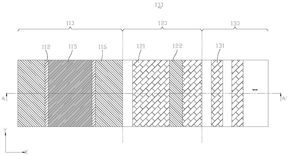
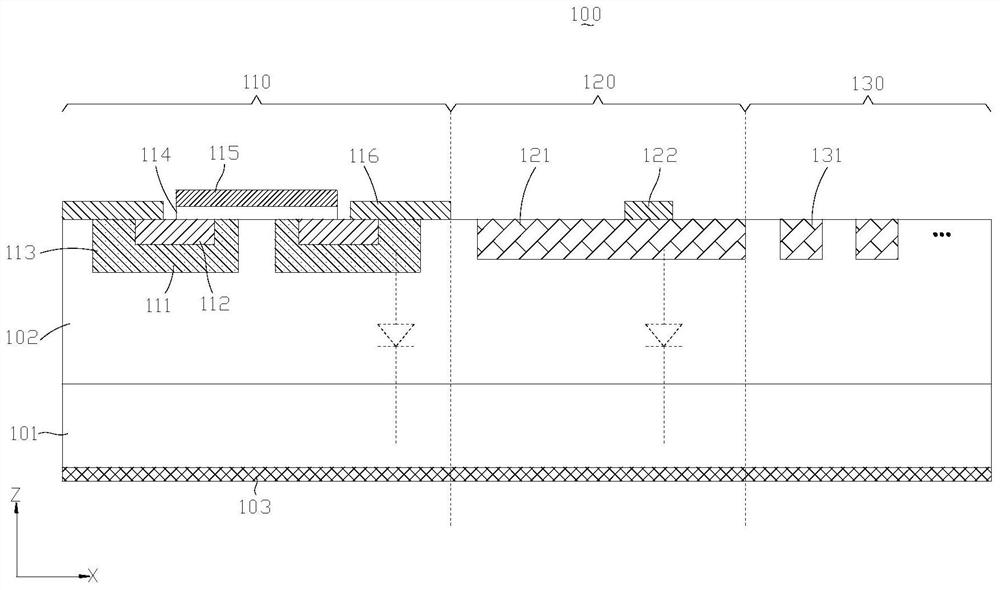
[0057] Such as image 3 and Figure 4 As shown, the embodiment of the present disclosure provides a silicon carbide MOSFET chip 200 with a planar gate structure, including a substrate 201 , a drift layer 202 , a drain metal layer 203 , an active region 210 , a transition region 220 and a terminal region 230 .

[0058] Exemplarily, the substrate 201 is a silicon carbide substrate of the first conductivity type.

[0059] The drift layer 202 is a drift layer of the first conductivity type and is located above the substrate 201 . The doping concentration and thickness of the drift layer 202 are adjusted according to different withstand voltage capabilities of the chip.

[0060] The drain metal layer 203 is located under the substrate 201 and forms an ohmic contact with the substrate 201 .

[0061] The active region 210 , the transition region 220 and the termination region 230 are all disposed on the drift layer 202 , and the transition region 220 is located between the active ...

Embodiment 2

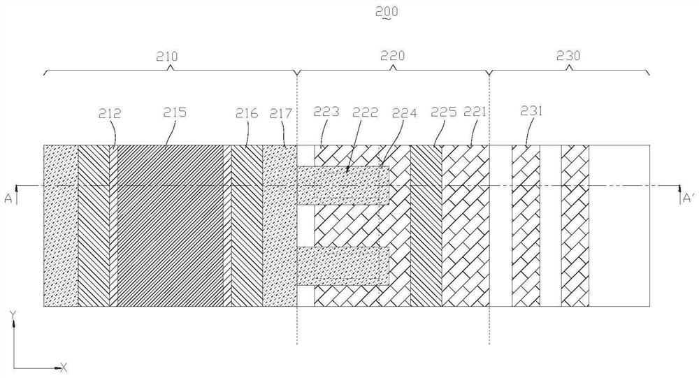
[0080] Such as Figure 5 and Figure 6 As shown, the embodiment of the present disclosure provides a silicon carbide MOSFET chip 300 with a planar gate structure, including a substrate 301 , a drift layer 302 , a drain metal layer 303 , an active region 310 , a transition region 320 and a terminal region 330 .

[0081] Exemplarily, the substrate 301 is a silicon carbide substrate of the first conductivity type.

[0082]The drift layer 302 is a drift layer of the first conductivity type and is located above the substrate 301 . The doping concentration and thickness of the drift layer 302 are adjusted according to different withstand voltage capabilities of the chip.

[0083] The drain metal layer 303 is located under the substrate 301 and forms an ohmic contact with the substrate 301 .

[0084] The active region 310 , the transition region 320 and the termination region 330 are all disposed on the drift layer 302 , and the transition region 320 is located between the active ...

Embodiment 3

[0098] Such as Figure 9 and Figure 10 As shown, the embodiment of the present disclosure provides a silicon carbide MOSFET chip 400 with a trench gate structure, including a substrate 401 , a drift layer 402 , a drain metal layer 403 , an active region 410 , a transition region 420 and a terminal region 430 .

[0099] Exemplarily, the substrate 401 is a silicon carbide substrate of the first conductivity type.

[0100] The drift layer 402 is a drift layer of the first conductivity type and is located above the substrate 401 . The doping concentration and thickness of the drift layer 402 are adjusted according to different withstand voltage capabilities of the chip.

[0101] The drain metal layer 403 is located under the substrate 401 and forms an ohmic contact with the substrate 401 .

[0102] The active region 410 , the transition region 420 and the termination region 430 are all disposed on the drift layer 402 , and the transition region 420 is located between the activ...


PUM

PropertyMeasurementUnit
thicknessaaaaaaaaaa

Abstract

The invention provides a silicon carbide MOSFET (metal oxide semiconductor field effect transistor) chip. The silicon carbide MOSFET chip comprises an active region, a terminal region and a transition region which are arranged on a drift layer, wherein the active region comprises a plurality of cellular structures; the cellular structure includes a second conductivity type first enhancement region disposed side by side with a source region in the surface of a first well region and in contact with one end of the source region away from the center of the cellular structure, and a first Schottky metal layer located above the drift layer on both sides of the cellular structure and forming Schottky contact with the drift layer. The transition region comprises a second source electrode metal layer which is arranged above the second enhancement region and forms ohmic contact with the second enhancement region, and a second Schottky metal layer which forms Schottky contact with a region, which is not covered by the second enhancement region, of the drift layer is arranged on the surface of the drift layer. By simultaneously integrating the SBD in the active region and the transition region of the silicon carbide MOSFET chip, the bipolar degradation effect of the silicon carbide chip is improved, and the reliability of the chip is improved.

Description

technical field [0001] The present disclosure relates to the technical field of semiconductor devices, in particular to a silicon carbide MOSFET chip. Background technique [0002] Silicon carbide (SiC) is a new wide-bandgap semiconductor material with excellent physical, chemical and electrical properties. The breakdown electric field strength of silicon carbide is 10 times that of traditional silicon, the thermal conductivity is 3 times that of silicon, and it has a higher switching frequency, which can reduce the loss and volume of energy storage components in the circuit. Theoretically, SiC devices can work in a high-temperature environment above 600 degrees Celsius, and have excellent radiation resistance, which greatly improves their high-temperature stability. [0003] However, limited by the existing manufacturing technology, the "bipolar degeneration" phenomenon in silicon carbide bipolar devices, that is, recombination after carrier injection (or excitation), a si...

Claims


Application Information

Patent Timeline
Patent Type & Authority Applications(China)
IPC IPC(8): H01L29/78H01L29/24H01L29/06
CPCH01L29/7827H01L29/24H01L29/0603Y02B70/10
Inventor 王亚飞陈喜明刘锐鸣赵艳黎李诚瞻罗海辉
Owner ZHUZHOU CRRC TIMES SEMICON CO LTD
Why Eureka
Try Eureka