Method for metallizing and electroplating only hole wall

A hole metallization and metallization technology is applied in the field of circuit board manufacturing technology to achieve the effects of simple hole metallization, good effect and reduced manufacturing cost

Active Publication Date: 2021-06-29
德中(天津)技术发展股份有限公司
View PDF11 Cites 11 Cited by
  • Summary
  • Abstract
  • Description
  • Claims
  • Application Information

AI Technical Summary

Problems solved by technology

[0023] In view of this, aiming at the defect that the prior art cannot independently metallize and electroplate to thicken the hole wall, and aiming at the deficiency of the new technical solution of the polymer film direct electroplating method, the present invention aims to propose a method for only metallizing and electroplating the hole wall. The electroplating method uses a non-photosensitive porous metallization active material ...

Method used


Image

  • Method for metallizing and electroplating only hole wall
  • Method for metallizing and electroplating only hole wall
  • Method for metallizing and electroplating only hole wall

Examples


Embodiment 1

[0086] This embodiment takes a double-sided printed circuit board as an example, and the specific processing steps are as follows:

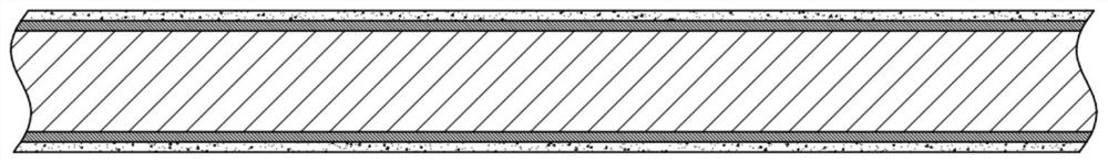
[0087] (1) Deposit parylene on the entire double-sided printed circuit board to form a masking layer 1, such as figure 1 as shown,

[0088] Specifically, the parylene coating produced by Xiayu Nanotechnology was deposited on the surface of the double-sided circuit board by vacuum vapor deposition, and the thickness of the coating was about 3um.

[0089] The prior art generally uses photo-induced dry film as an anti-plating mask. The photo-induced dry film has a three-layer structure. The photosensitive adhesive coating is between the carrier film and the protective film and is composed of adhesive and photopolymerizable monomer. It is complicated, and it needs to go through the process of photo-drawing, filming, exposure, and development; moreover, it is expensive, the strength is not high, and the thickness is relatively large, generally above...

Embodiment 2

[0119] This embodiment takes a 4-layer printed circuit board as an example, and the specific processing steps are as follows:

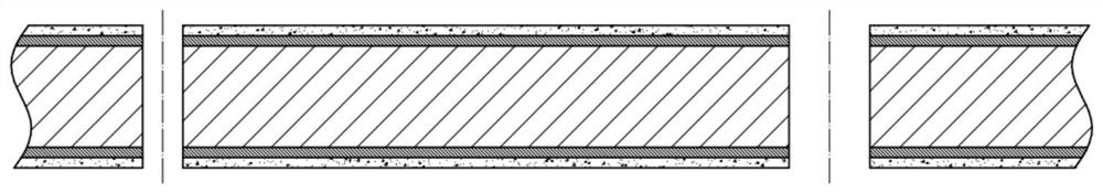
[0120] (1) On the 4-layer circuit board that has completed the inner layer circuit and laminated, double-sided heat-pressed composite RPP film, such as Figure 7 shown.

[0121] Specifically, heat-press composite RPP film, the thickness of the film is about 10um, and the bonding parameters are: pressure 15kg / cm 2 , temperature 100°C, speed 0.1m / min.

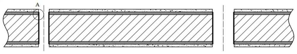
[0122] (2) After direct laser drilling or mechanical drilling, the laser is used to remove the slag on the hole wall, such as Figure 8 shown.

[0123] Specifically, in this embodiment, the hole is mechanically drilled first, and then the hole is expanded by a femtosecond laser beam, so as to finally meet the aperture requirement. The mechanical drilling uses the DCT-DM350 equipment produced by Dezhong Technology Co., Ltd. to drill holes according to the design requirements. Import the designed data...


PUM

PropertyMeasurementUnit
Thicknessaaaaaaaaaa
Thicknessaaaaaaaaaa
Thicknessaaaaaaaaaa

Abstract

The invention provides a method for metallizing and electroplating only a hole wall. The method comprises the following steps of coating a material of a sparse-hole metallization active substance on a copper-clad plate to mask the plate surface, drilling a hole, only activating the hole wall, and only directly electroplating or firstly carrying out chemical plating and then electroplating the hole wall to the required thickness. The material adopted by the invention has the performance of the sparse-hole metallization active substance, the plate surface is masked, metal is only deposited on the hole wall, the thickness of a plating layer is easy to control, the quality of the metallization hole is better, the circuit board can better meet the electrical requirements, finer conductive patterns can be manufactured, the cost is reduced, and the method is environment-friendly. The method is suitable for mass production of various circuit boards, and is further suitable for small-batch and multi-variety production of circuit board samples.

Description

technical field [0001] The invention relates to the field of circuit board manufacturing technology, in particular to a method for metallizing and electroplating only hole walls. Background technique [0002] In today's world, electronics are everywhere. One of the most important components of electronic products is the circuit board, which is the electrical connection channel between various components and determines their respective electrical parameters and electrical logic relationships; at the same time, it is also the installation and fixed carrier of each component, and is the skeleton. Among them, the electrical connection channel is realized by conductive patterns and metallized holes. Solderability development of solder patterns and solder areas. However, in the traditional method of making circuit boards, the manufacture of conductive patterns and solder resist patterns is completed by pattern transfer, and the manufacture of metallized holes requires substrate...

Claims


Application Information

Patent Timeline
IPC IPC(8): H05K3/42H05K3/00
CPCH05K3/42H05K3/0026H05K3/0055H05K3/423H05K2203/0562H05K2203/0703H05K2203/107
Inventor 胡宏宇宋金月于跃欣
Owner 德中(天津)技术发展股份有限公司
Why Eureka
Try Eureka