Silicon carbide substrate annealing process and silicon carbide substrate annealing equipment

A technology of silicon carbide substrate and annealing process, applied in the direction of electrical components, semiconductor/solid-state device manufacturing, circuits, etc., can solve the problems of SiC surface roughening, increasing process time consumption and tape-out cost

Inactive Publication Date: 2021-07-02
GREE ELECTRIC APPLIANCES INC
View PDF4 Cites 0 Cited by
  • Summary
  • Abstract
  • Description
  • Claims
  • Application Information

AI Technical Summary

Problems solved by technology

But at the same time, the high temperature will cause the Si atoms in SiC to evaporate, making the surface of S...

Method used


Image

  • Silicon carbide substrate annealing process and silicon carbide substrate annealing equipment
  • Silicon carbide substrate annealing process and silicon carbide substrate annealing equipment
  • Silicon carbide substrate annealing process and silicon carbide substrate annealing equipment

Examples


Embodiment Construction

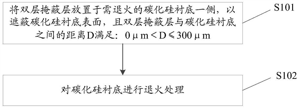
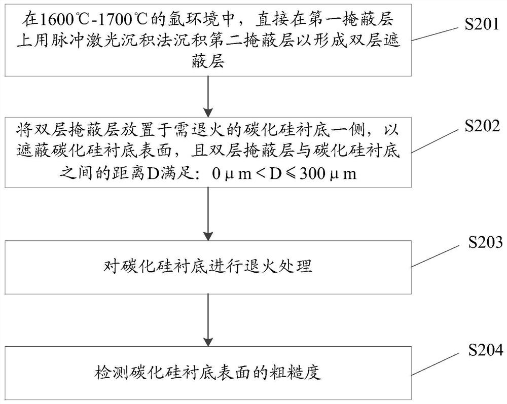
[0032] In order to solve this problem, the industry proposes a solution to the Si atom evaporation phenomenon that occurs during the annealing of p-type (Al ion implantation to SiC to achieve p-type doping) SiC substrate: PLD (pulsed laserdeposition) on the surface of p-type SiC Pulse laser deposition) first deposit a layer of AlN masking layer on the surface of SiC, and then deposit a layer of BN masking layer on the surface of AlN. After annealing, the double masking layer AlN / BN needs to be removed. BN is removed by ion bombardment first, and then AlN is corroded by KOH solution. These two removal steps not only increase the process time, but also increase the tape-out cost. This patent proposes an improved method for SiC annealing AlN / BN double-layer masking, which can not only significantly reduce the time consumption of the process, but also reduce the cost. The following will clearly and completely describe the technical solutions in the embodiments of the present...


PUM

PropertyMeasurementUnit
Thicknessaaaaaaaaaa
Thicknessaaaaaaaaaa

Abstract

The invention relates to the field of semiconductors, and discloses a silicon carbide substrate annealing process and silicon carbide substrate annealing equipment. The silicon carbide substrate annealing process specifically comprises the steps that double masking layers are placed on one side of a silicon carbide substrate needing to be annealed so as to shield the surface of the silicon carbide substrate, the distance D between the double masking layers and the silicon carbide substrate is more than 0 [mu] m and less than or equal to 300 [mu] m; and the silicon carbide substrate is annealed. The distance between the silicon carbide substrate and the double-layer masking layer can be adjusted, so that the purpose of improving the surface roughness of the silicon carbide substrate is achieved. Therefore, after the silicon carbide substrate is annealed, a complicated masking layer removal process is not needed, and only the double masking layers need to be directly taken away, so that the process is optimized to reduce the process cost under the condition of ensuring the same effect.

Description

technical field [0001] The invention relates to the technical field of semiconductors, in particular to a silicon carbide substrate annealing process and silicon carbide substrate annealing equipment. Background technique [0002] As a third-generation new semiconductor, silicon carbide (SiC) has the characteristics of wide bandgap, high critical breakdown electric field, and high thermal conductivity. Compared with traditional silicon carbide, it is used in high temperature, high pressure, high frequency, high power and other fields. base devices have great advantages. [0003] Due to the special material of SiC devices, there are many differences in process compared with traditional Si. Due to the large bond energy of SiC and the low solid solubility of impurities in SiC, the diffusion process cannot achieve n-type or p-type doping, and ion implantation is the only way to achieve SiC doping. Due to the high energy and large dose of the ion implantation process, it will d...

Claims


Application Information

Patent Timeline
IPC IPC(8): H01L21/324H01L21/67
CPCH01L21/324H01L21/67098
Inventor 林苡任史波陈道坤曾丹
Owner GREE ELECTRIC APPLIANCES INC
Why Eureka
Try Eureka