
Preparation method of perovskite thin film and perovskite LED

A perovskite and thin film technology, applied in the field of optoelectronic materials, can solve the problems of poor film quality and weak luminous intensity, and achieve the effects of high brightness, smooth surface and improved lifespan

Pending Publication Date: 2021-07-02
INST OF SEMICONDUCTORS - CHINESE ACAD OF SCI
View PDF0 Cites 0 Cited by
  • Summary
  • Abstract
  • Description
  • Claims
  • Application Information

AI Technical Summary

Problems solved by technology

[0006] In view of the above problems, the present disclosure provides a method for preparing a perovskite thin film and a perovskite LED, which are used to at least partially solve the technical problems of weak luminous intensity and poor film quality in traditional methods

Method used


Image

  • Preparation method of perovskite thin film and perovskite LED
  • Preparation method of perovskite thin film and perovskite LED
  • Preparation method of perovskite thin film and perovskite LED

Examples


preparation example Construction

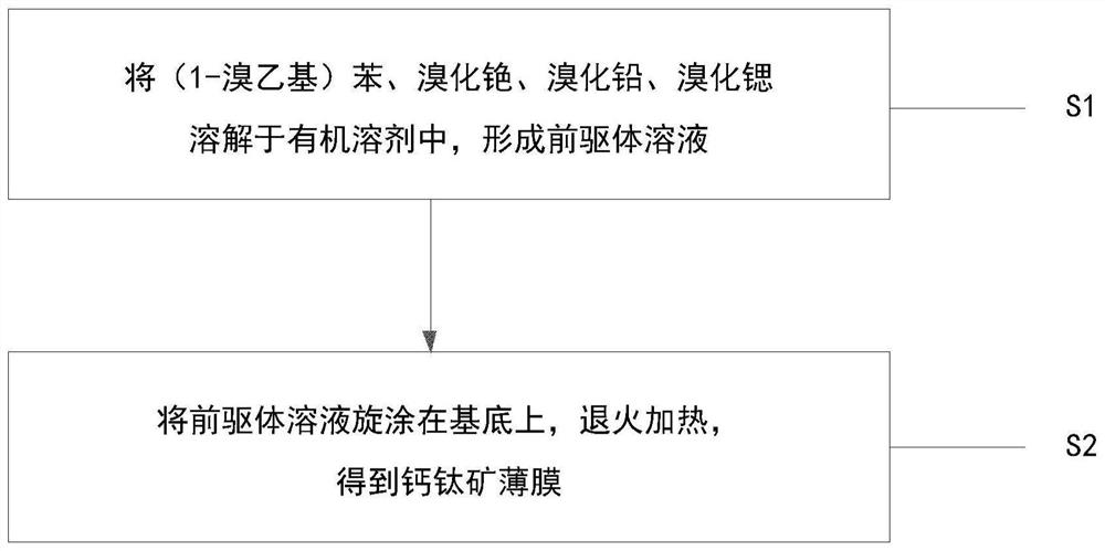
[0029] Embodiments of the present disclosure provide a method for preparing a perovskite thin film, please refer to figure 1 , including: S1, dissolving (1-bromoethyl)benzene, cesium bromide, lead bromide, and strontium bromide in an organic solvent to form a precursor solution; S2, spin-coating the precursor solution on the substrate, annealing Heating to obtain a perovskite film.

[0030] (1-Bromoethyl) benzene, also known as PEABr, has the following structural formula as formula I:

[0031]

[0032] Due to the addition of PEABr, a quasi-two-dimensional perovskite structure is formed, and the size of the perovskite crystal decreases; with the increase of PEAr, the proportion of the quasi-two-dimensional perovskite structure with a larger band gap increases in the perovskite film , the energy transition of excitons from a large bandgap crystal structure to a low bandgap crystal structure is more likely to occur, non-radiative recombination is suppressed, radiative recombi...

Embodiment 1

[0074] A method for preparing a perovskite film with high luminous intensity, the steps are as follows:

[0075] (1) Preparation of perovskite precursor solution (ie S1): the molar ratio is PEABr: CsBr: PbBr 2 :SrBr 2 =1:1:A:B was dissolved in dimethyl sulfoxide, stirred evenly to prepare a clear and transparent perovskite precursor solution, wherein the value of A was 1.52, the value of B was 0, and the value of dimethyl sulfoxide The volume is 1mL, PbBr 2 The molar mass is 0.5mM.

[0076] (2) Preparation of PEDOT:PSS layer: PEDOT:PSS and anhydrous isopropanol are prepared in a volume ratio of 10:1 to form a PEDOT:PSS mixed solution, stirred evenly at low temperature, and filtered using a water-based filter with a pore size of 0.22 or 0.45 μm Does not dissolve small particles.

[0077] The spin coating of PEDOT:PSS layer is divided into three stages, the first stage rotation speed is 1200rpm, time is 12s, acceleration 500rpm / s; The second stage rotation speed is 2000rpm, ...

Embodiment 2

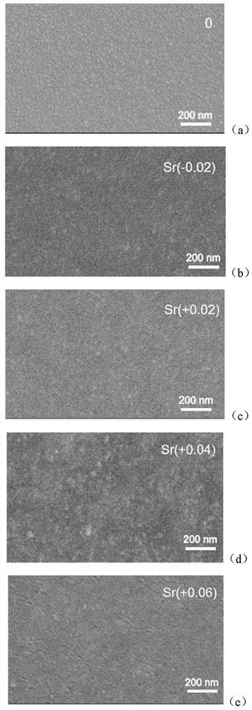
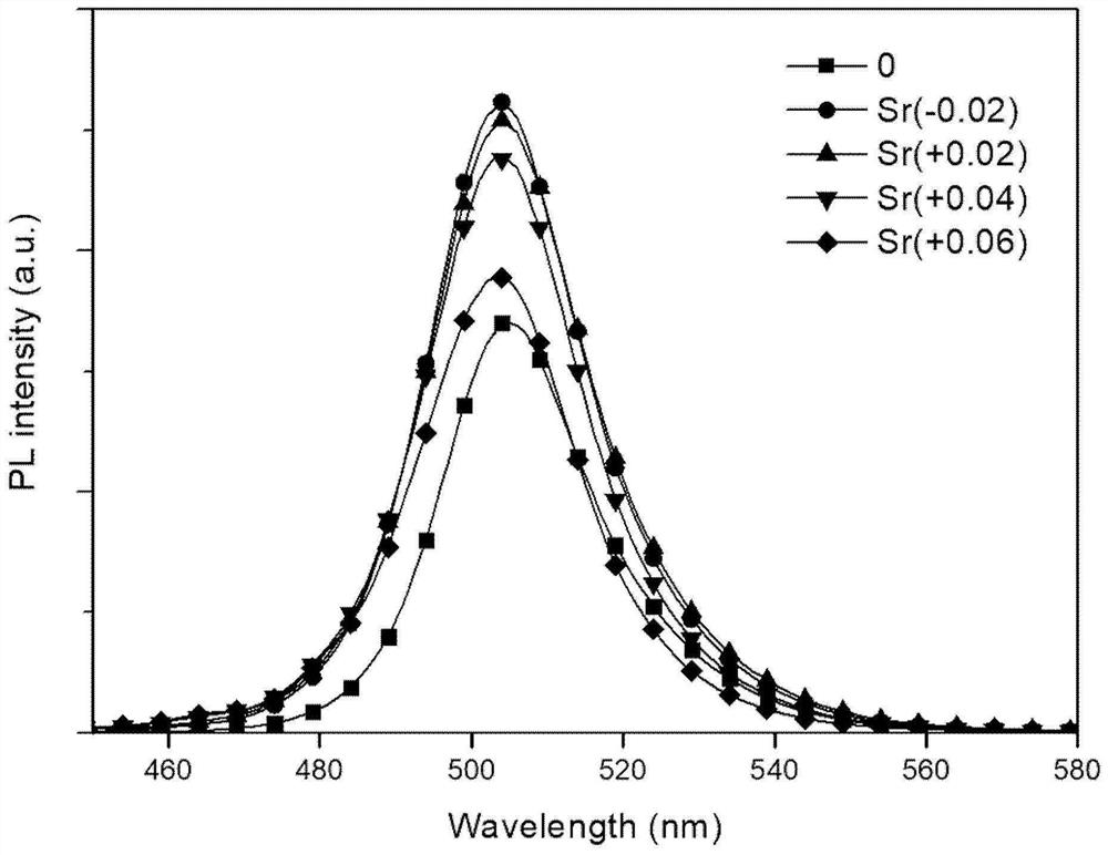
[0082] The difference with Example 1 is: in step (1), the value of A in the perovskite thin film precursor solution is prepared to be 1.46, the value of B is 0.06, and the value of PbBr 2 The molar mass is 0.48mM, and others are all the same as in Example 1. We define this sample label as Sr(-0.02), see figure 2 Middle (b) diagram.


PUM

PropertyMeasurementUnit
Thicknessaaaaaaaaaa
Thicknessaaaaaaaaaa
Thicknessaaaaaaaaaa

Abstract

The invention provides a preparation method of a perovskite thin film, and the method comprises the following steps: S1, dissolving (1-bromoethyl) benzene, cesium bromide, lead bromide and strontium bromide in an organic solvent to form a precursor solution; S2, spin-coating a substrate with the precursor solution, and annealing and heating to obtain the perovskite thin film. The method disclosed by the invention is simple to operate and short in preparation time, and the photoluminescence intensity of the film is obviously improved. The invention further provides a perovskite LED.

Description

technical field [0001] The disclosure relates to the technical field of optoelectronic materials, in particular to a method for preparing a perovskite thin film and a perovskite LED. Background technique [0002] As a direct bandgap semiconductor material, perovskite materials have gradually become excellent solid luminescent materials due to their excellent properties such as simple preparation process, high carrier mobility, long carrier lifetime and adjustable bandgap. Alternatives, its application in the field of light-emitting diodes has also become a research hotspot. [0003] At present, the highest external quantum efficiencies of green, red, and blue perovskite LEDs have been greatly improved. Since external quantum efficiency is an important indicator for measuring the performance of light-emitting diodes, many studies have focused on how to improve external quantum efficiency. Studies based on the influence of perovskite thin films on the lifetime of perovskite L...

Claims


Application Information

Patent Timeline
IPC IPC(8): H01L51/56H01L51/50H01L51/54
CPCH10K71/12H10K71/40H10K85/6572H10K85/657H10K50/11H10K71/00
Inventor 陈丹刘陶然左玉华郑军刘智成步文
Owner INST OF SEMICONDUCTORS - CHINESE ACAD OF SCI
Learn More