

Current type CdZnTe detector with strip-shaped electrode structure and preparation method of current type CdZnTe detector
A strip-shaped electrode and current-type technology, applied in the direction of circuits, electrical components, semiconductor devices, etc., can solve the problems of slow response speed and low response amplitude of pulsed X-rays, and achieve carrier drift and recombination speed acceleration, response The effect of large amplitude and large sensitive volume
- Summary
- Abstract
- Description
- Claims
- Application Information
AI Technical Summary
Problems solved by technology
Method used
Image

Examples
preparation example Construction
[0053] A kind of preparation method of the current type CdZnTe detector of above-mentioned strip electrode structure: comprise the following steps:
[0054] 1) modeling
[0055] Using the finite element software COMSOL to build a model, design amperometric CdZnTe detectors with different electrode sizes;
[0056] 2) Field analysis and size determination
[0057] 2.1) Establish an electrostatic physical field for the current-type CdZnTe detector models with different electrode sizes constructed in step 1), and adopt free tetrahedral grid division, and some grid unit sizes are calibrated as semiconductor conventional divisions;
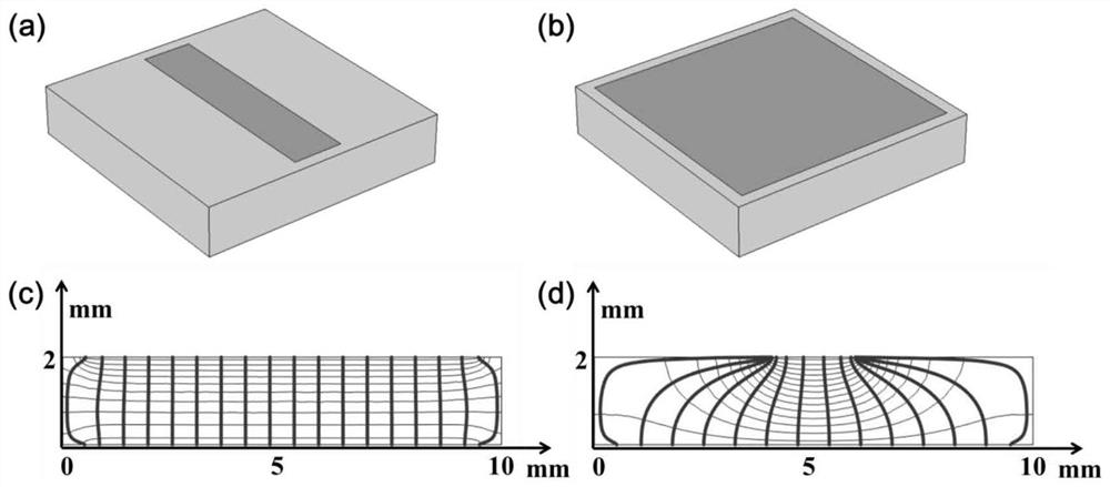
[0058] 2.2) Carry out model calculation to the internal electric field distribution and electric field strength of different electrode size current-type CdZnTe detector models, analyze the distribution of each detector's internal weight potential field; select a detector model that meets the requirements, and determine the size; figure 1 As shown, the...
Embodiment 1
[0060] After the previous steps, determine the following dimensions:
[0061] CdZnTe crystal size is 10×10×2mm 3 , the strip electrode size is 2×9mm 2 , the size of the plane electrode on the other side is 9×9mm 2
[0062] 3) Pretreatment
[0063] 3.1) Cut the CdZnTe crystal into a size of 10×10×2mm 3 Wafers, and screen out the Te inclusion phase size is less than 10μm, the density is less than 10 4 / cm 2 , and uniformly distributed wafers;
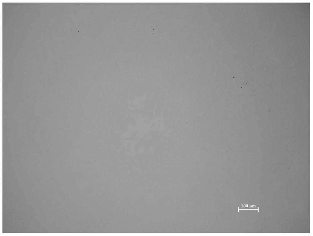
[0064] 3.2) Mechanically polish the wafer obtained in step 3.1, and throw it until there is no scratch under a 100-fold optical microscope;
[0065] 3.3) Eliminate the stress damage layer on the wafer surface after mechanical polishing in step 3.2) by chemical etching, specifically:
[0066] Bromomethanol solution with a volume fraction of 2% was used as the chemical etching solution. Firstly, the wafer was cleaned in the methanol solution, and then the wafer was clamped with tweezers and immersed in the bromomethanol solution and...
Embodiment 2
[0079] After the previous steps, determine the following dimensions:
[0080] CdZnTe crystal size is 10×10×2mm 3 , the strip electrode size is 1×9mm 2 , the size of the plane electrode on the other side is 9×9mm 2
[0081] 3) Pretreatment
[0082] 3.1) Cut the CdZnTe crystal into a size of 10×10×2mm 3 Wafers, and screen out the Te inclusion phase size is less than 10μm, the density is less than 10 4 / cm 2 , and uniformly distributed wafers;
[0083] 3.2) Mechanically polish the wafer obtained in step 3.1, and throw it until there is no scratch under a 100-fold optical microscope;
[0084] 3.3) Eliminate the stress damage layer on the wafer surface after mechanical polishing in step 3.2) by chemical etching, specifically:
[0085] Using bromomethanol solution with a volume fraction of 2% as the chemical etching solution, first clean the wafer in methanol solution, then clamp the wafer with tweezers and immerse it in bromomethanol solution and move it up and down for 70s...
PUM
| Property | Measurement | Unit |
|---|---|---|
| size | aaaaa | aaaaa |
| thickness | aaaaa | aaaaa |
| current | aaaaa | aaaaa |
Abstract
Description
Claims
Application Information