Silicon-containing monomer, photocuring composition, packaging structure and semiconductor device
A silicon monomer, photocuring technology, applied in semiconductor devices, semiconductor/solid-state device manufacturing, electric solid-state devices, etc., can solve the problems of water vapor transmittance angle, low light transmittance, etc., and achieve low water vapor transmission rate, high light transmittance, and high curing speed
- Summary
- Abstract
- Description
- Claims
- Application Information
AI Technical Summary
Problems solved by technology
Method used
Image

Examples
Embodiment 1
[0033] This embodiment provides a method for preparing a packaging structure, which includes the following steps:
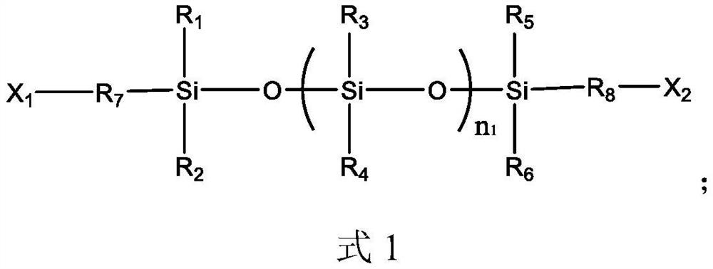
[0034] S1. Weigh 20g of silicon-containing monomer 001, 75g of epoxy alkyl-containing diluent L001 and 5g of diaryliodonium salt, mix them together, stir at 50°C for 80h under vacuum, and then filter with a syringe filter, and use a particle counter to detect, when the number of particles with a particle size greater than 0.5 μm is detected to be no more than 50, the photocurable composition is obtained for use; wherein, the structural formula of the silicon-containing monomer 001 is as follows:
[0035]
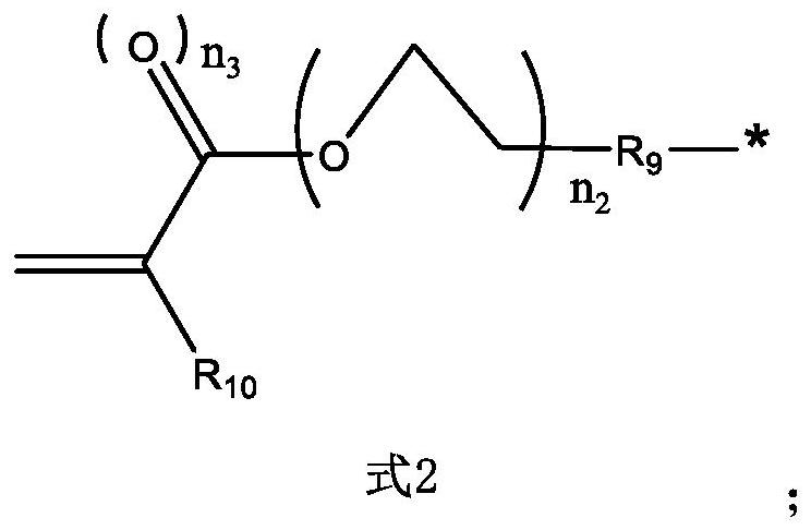
[0036] The structural formula of the alkylene oxide diluent L001 is as follows:
[0037]
[0038] S2. Selecting silicon nitride as the inorganic layer material, and coating the inorganic layer material on the surface of the object to be packaged by chemical vapor deposition (Chemical Vapor Deposition, CVD) to form an inorganic layer.
[0039] S3. Spray t...
Embodiment 2
[0042] This embodiment provides a method for preparing a packaging structure, which includes the following steps:
[0043] S1. Weigh 20g of silicon-containing monomer 002, 75g of epoxy alkyl-containing diluent L002 and 5g of triarylsulfonium salt, mix them together, stir at 50°C for 80h under vacuum, and then use a syringe filter Filter, use a particle counter to detect, when the number of particles with a particle size greater than 0.5 μm is detected to be no more than 50, obtain a photocurable composition for use; wherein, the structural formula of the silicon-containing monomer 002 is as follows:
[0044]
[0045] The structural formula of the alkylene oxide diluent L002 is as follows:
[0046]
[0047] S2. Selecting silicon nitride as the inorganic layer material, and coating the inorganic layer material on the surface of the object to be packaged by chemical vapor deposition (Chemical Vapor Deposition, CVD) to form an inorganic layer.
[0048] S3. Spray the above-men...
Embodiment 3
[0051] This embodiment provides a method for preparing a packaging structure, which includes the following steps:
[0052] S1. Weigh 20g of silicon-containing monomer 003, 75g of alkylene oxide-containing diluent L003 and 5g of iron arene salt photoinitiator, mix them together, stir for 80h under vacuum at 50°C, and then filter with a syringe filter, and use a particle counter to detect, when the number of particles with a particle size greater than 0.5 μm is detected to be no more than 50, the photocurable composition is obtained for use; wherein, the structural formula of the silicon-containing monomer 003 is as follows:
[0053]
[0054] The structural formula of the alkylene oxide diluent L003 is as follows:
[0055]
[0056] S2. Selecting silicon nitride as the inorganic layer material, and coating the inorganic layer material on the surface of the object to be packaged by chemical vapor deposition (Chemical Vapor Deposition, CVD) to form an inorganic layer.
[005...
PUM
| Property | Measurement | Unit |
|---|---|---|
| Particle size | aaaaa | aaaaa |
Abstract
Description
Claims
Application Information
 - R&D
- Intellectual Property
- Life Sciences
- Materials
- Tech Scout
- Unparalleled Data Quality
- Higher Quality Content
- 60% Fewer Hallucinations
Browse by: Latest US Patents, China's latest patents, Technical Efficacy Thesaurus, Application Domain, Technology Topic, Popular Technical Reports.
© 2025 PatSnap. All rights reserved.Legal|Privacy policy|Modern Slavery Act Transparency Statement|Sitemap|About US| Contact US: help@patsnap.com