POLO-IBC solar cell and preparation method thereof

A solar cell and electrode technology, applied in the field of solar cells, can solve the problems of high cost, complicated process, and long production cycle, and achieve the effects of reducing processes and steps, simple process, and shortening the production cycle

Active Publication Date: 2021-08-06
ZHEJIANG AIKO SOLAR ENERGY TECH CO LTD +2
View PDF13 Cites 2 Cited by
  • Summary
  • Abstract
  • Description
  • Claims
  • Application Information

AI Technical Summary

Problems solved by technology

This method requires ion implantation equipment to form P + Poly-Si layer and N + Ploy-Si layer, high cost
[0005] A method for preparing an IBC solar cell disclosed in Chinese patent CN110112255A needs to be formed through multiple masks, the process is complicated, and the production cycle is long

Method used


Image

  • POLO-IBC solar cell and preparation method thereof
  • POLO-IBC solar cell and preparation method thereof

Examples


preparation example Construction

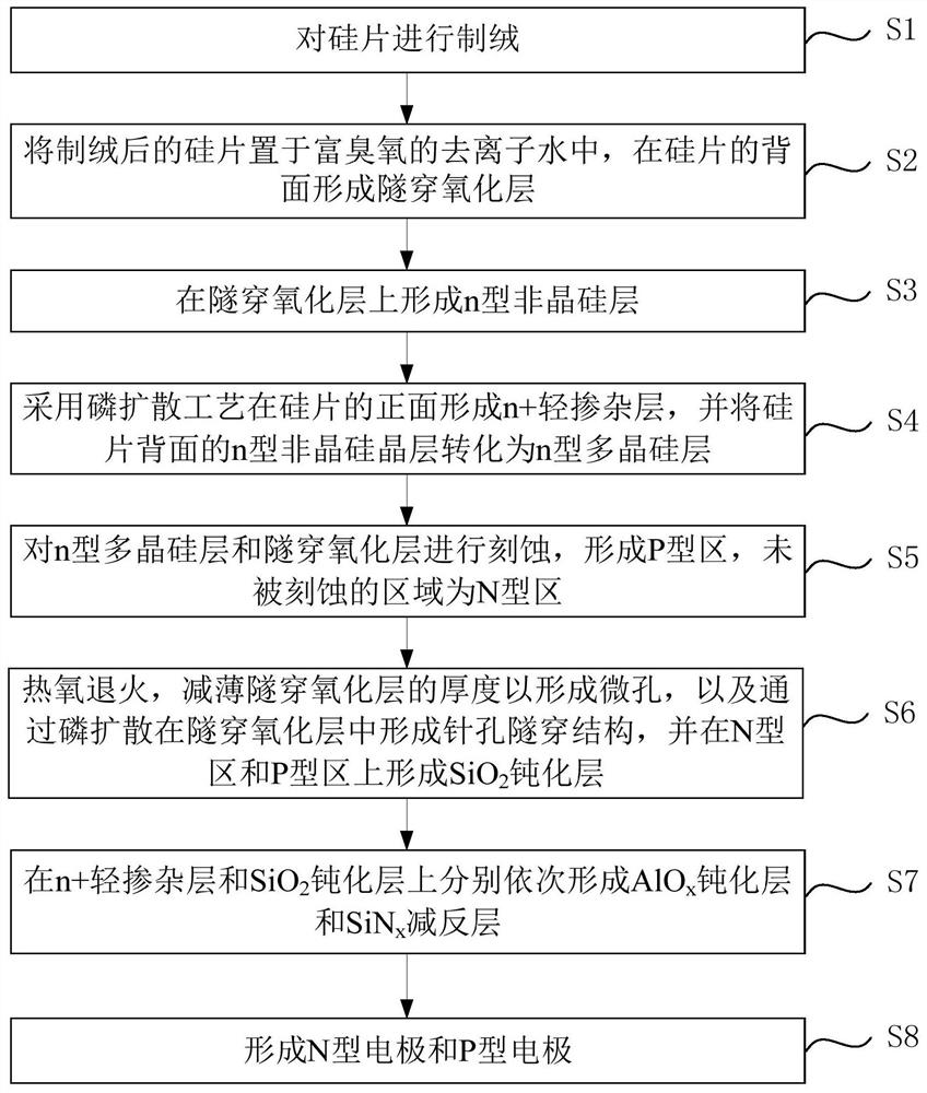
[0037] see figure 1 , the preparation method of a kind of POLO-IBC solar cell provided by the invention, comprises the following steps:

[0038] S1. Texturing the silicon wafer;

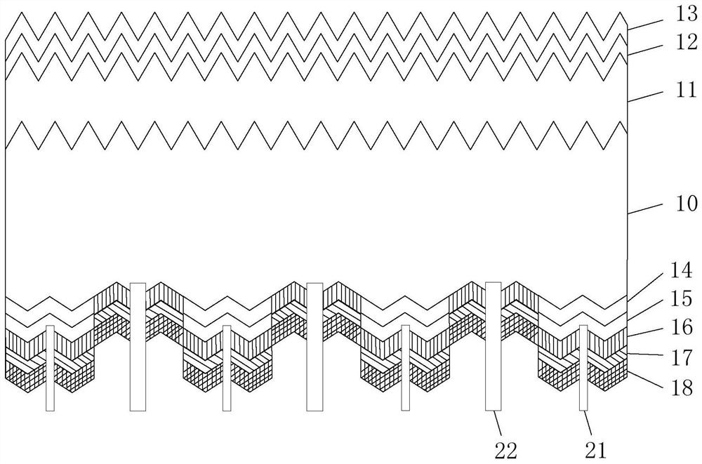
[0039] Specifically, the silicon wafer is a P-type silicon wafer with a thickness of 50-200 μm, a resistivity of 0.3-10 Ω·cm, a minority carrier lifetime of 0.2-2 ms, and a pyramidal light-trapping structure formed on the surface of the silicon wafer after texturing.

[0040] S2, placing the textured silicon wafer in ozone-rich deionized water to form a tunnel oxide layer on the back side of the silicon wafer;

[0041] Specifically, the textured silicon wafer is placed in ozone-rich deionized water for 1-30 minutes, and a tunnel oxide layer with a thickness of 0.5-2.5 nm is formed on the back surface of the silicon wafer. Wherein the tunnel oxide layer is SiO 2 layer.

[0042] Preferably, the temperature of the ozone-enriched deionized water is 15-60°C.

[0043]It should be noted that the ozone-...

Embodiment 1

[0079] S1. Texturing a silicon wafer, the silicon wafer is a P-type silicon wafer with a size of 166mm*166mm, a thickness of 160μm, a resistivity of 2.0Ω·cm, and a minority carrier lifetime of 1ms;

[0080] S2. Place the textured silicon wafer in ozone-rich deionized water for 15 minutes to form a tunneling oxide layer with a thickness of 1.5 nm on the back side of the silicon wafer;

[0081] S3, adopt CVD equipment, pass into PH 3 、SiH 4 and N 2 gas, at a temperature of 450°C, deposit and form an n-type amorphous silicon layer on the tunnel oxide layer, and the doping concentration of the n-type amorphous silicon layer is 4*10 20 cm -3 , with a thickness of 180nm;

[0082] S4. Place the silicon wafer in the diffusion equipment, feed the phosphorus source into the diffusion equipment, and diffuse for 80 minutes at a temperature of 850°C, wherein the back of the silicon wafer leans against the boat, and the front faces the phosphorus source (POCl 3 ), forming an n+ lightly ...

Embodiment 2

[0089] S1, same as step S1 of embodiment 1;

[0090] S2. Place the textured silicon wafer in ozone-rich deionized water for 20 minutes to form a tunneling oxide layer with a thickness of 2.0 nm on the back side of the silicon wafer;

[0091] S3, adopt CVD equipment, pass into PH 3 、SiH 4 and N 2 gas, at a temperature of 550°C, deposit and form an n-type amorphous silicon layer on the tunnel oxide layer, and the doping concentration of the n-type amorphous silicon layer is 3*10 20 cm -3 , with a thickness of 300nm;

[0092] S4. Place the silicon wafer in the diffusion equipment, feed the phosphorus source into the diffusion equipment, and diffuse for 75 minutes at a temperature of 950°C, wherein the back of the silicon wafer leans against the boat, and the front faces the phosphorus source (POCl 3 ), forming an n+ lightly doped layer on the front side of the silicon wafer, and converting the n-type amorphous silicon layer on the back side of the silicon wafer into an n-ty...


PUM

PropertyMeasurementUnit
thicknessaaaaaaaaaa
depthaaaaaaaaaa
thicknessaaaaaaaaaa

Abstract

The invention discloses a POLO-IBC solar cell and a preparation method thereof. The method comprises the following steps of: S1, texturing a silicon wafer; S2, forming a tunneling oxide layer on the back surface of the silicon wafer; S3, forming an n-type amorphous silicon layer on the tunneling oxide layer; S4, forming an n + lightly doped layer on the front surface of the silicon wafer, and converting the n-type amorphous silicon layer on the back surface of the silicon wafer into an n-type polycrystalline silicon layer; S5, forming a P-type region and an N-type region; S6, performing thermal oxygen annealing; S7, respectively forming an AlOx passivation layer and a SiNx antireflection layer on the n + lightly doped layer and a SiO2 passivation layer in sequence; and S8, forming an N-type electrode and a P-type electrode. The preparation method is simple in process, short in production period and low in cost.

Description

technical field [0001] The invention relates to the technical field of solar cells, in particular to a POLO-IBC solar cell and a preparation method thereof. Background technique [0002] At present, the efficiency improvement of PERC cells has gradually reached a bottleneck period, and client component manufacturers continue to have strong demand for high-efficiency cells. Interdigitated Back Contact (IBC) solar cells in high-efficiency cell structures have the advantages of high conversion efficiency, no frontal shielding, beautiful appearance, and simple and diverse component packaging. [0003] In the existing method, a passivation contact structure (POLy-Si on passedivatedinterfacial Oxides, POLO) is superimposed on the basis of the IBC structure to further improve the conversion efficiency of the battery. However, this method has complicated process, long production cycle and high cost, and cannot realize mass production. [0004] Chinese patent CN107342332A discloses...

Claims


Application Information

Patent Timeline
Patent Type & Authority Applications(China)
IPC IPC(8): H01L31/18H01L31/0216H01L31/0224H01L31/0288H01L31/0352
CPCH01L31/1804H01L31/02167H01L31/02168H01L31/022441H01L31/0288H01L31/0352Y02P70/50Y02E10/547
Inventor 李懋鸿陈刚
Owner ZHEJIANG AIKO SOLAR ENERGY TECH CO LTD
Why Eureka
Try Eureka