
Two-dimensional material resistive random access memory and preparation method thereof

A technology of two-dimensional materials and memristors, applied in the direction of electrical components, etc., can solve the problems of high manufacturing cost and poor quality, and achieve the effect of good uniformity, convenient preparation and simple preparation

Active Publication Date: 2021-08-10
GUILIN UNIV OF ELECTRONIC TECH
View PDF11 Cites 0 Cited by
  • Summary
  • Abstract
  • Description
  • Claims
  • Application Information

AI Technical Summary

Problems solved by technology

[0004] The purpose of the present invention is to provide a two-dimensional material resistive variable memory and its preparation method, aiming to solve the problems of high preparation cost and poor quality of two-dimensional material resistive variable memory in the prior art

Method used


Image

  • Two-dimensional material resistive random access memory and preparation method thereof
  • Two-dimensional material resistive random access memory and preparation method thereof
  • Two-dimensional material resistive random access memory and preparation method thereof

Examples


preparation example Construction

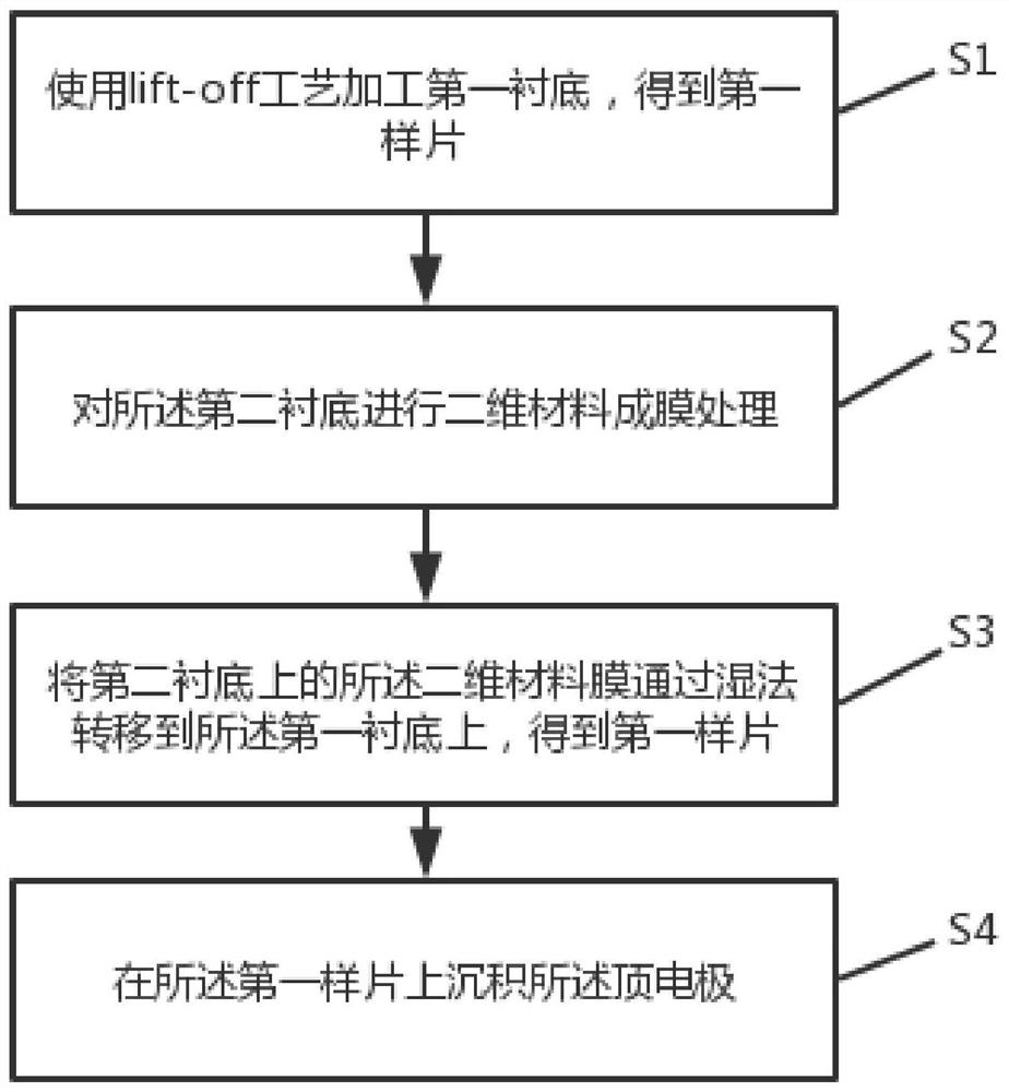
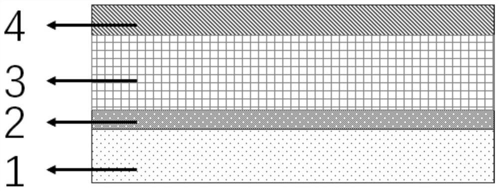
[0045] see Figure 1 to Figure 4 , the invention provides a method for preparing a two-dimensional material memristor, comprising the following steps:

[0046] S1: Process the first substrate by using a lift-off process to obtain a first sample;

[0047] S2: performing a two-dimensional material film forming process on the second substrate;

[0048] S3: transfer the two-dimensional material film on the second substrate to the sample by wet method to obtain a second sample;

[0049] S4: Depositing the top electrode on the second sample.

[0050] Specifically, the steps of processing the first substrate using the lift-off process to obtain the first sample include:

[0051] photoetching an electrode pattern on the first substrate;

[0052] Depositing a bottom electrode on the first substrate, and then leaving the bottom electrode on the first substrate by deglue treatment, to obtain a first sample.

[0053] Specifically, the electrode pattern is drawn on the first substrate...

specific Embodiment 1

[0067] The first substrate is an ITO glass substrate, and the ITO glass substrate is patterned on the surface by photolithography, 10 lines of 40 μm.

[0068] The bottom electrode is deposited on the ITO glass substrate by magnetron sputtering or evaporation evaporation process.

[0069] Take 1 g of hexagonal boron nitride powder and dimethylformamide to make a two-dimensional material suspension, and ultrasonicate in a water bath for 10 hours to obtain the first suspension.

[0070] Subsequently, 1 / 3 of the supernatant of the first suspension was taken and its concentration was determined by vacuum filtration.

[0071] Select 1cmx1cm copper foil as the second substrate, use a beaker as the container, fix the 1cmx1cm copper foil and the syringe hose in the middle of the beaker (100ml), add deionized water, and just submerge the 1cmx1cm copper foil by 0.5cm place.

[0072] Connect the syringe to the hose, slowly absorb the mixed solution, so that the liquid level of the mixed...


PUM

PropertyMeasurementUnit
Thicknessaaaaaaaaaa
Thicknessaaaaaaaaaa

Abstract

The invention discloses a two-dimensional material resistive random access memory and a preparation method thereof. Compared with a resistive random access memory prepared by chemical vapor deposition, the two-dimensional material resistive random access memory has the advantages of convenience in preparation, no dependence on equipment and the like, and has the advantages of good uniformity, good repeatability, simplicity in preparation and the like for resistive random access memories prepared by drip casting, spin coating and other methods. The two-dimensional material resistive random access memory prepared by the method disclosed by the invention shows a switch ratio of 6 orders of magnitude, has obvious advantages in comparison with 2-3 orders of magnitude shown by other traditional materials below dozens of nanometers, and is 4-5 orders of magnitude shown by a two-dimensional material resistive random access memory prepared based on a drop casting method and a spin coating method; under the conditions of simple preparation and low dependence on equipment, the on-off ratio similar to that of a two-dimensional material resistive random access memory (7 orders of magnitude) prepared by chemical vapor deposition can be achieved, and the resistive random access memory also has the potential of multi-stage storage under the high on-off ratio.

Description

technical field [0001] The invention relates to the field of resistive variable memory, in particular to a two-dimensional material resistive variable memory and a preparation method thereof. Background technique [0002] In today's era of information explosion, information storage has become a daily necessity for people. At present, mainstream memories, such as DRAM, SRAM and FLASH, all use transistors to build storage bits in their storage technologies. However, the size of CMOS technology has gradually approached its theoretical limit. size. As a result, resistive memory was born on demand. With its simple sandwich structure, the size of resistive memory can be reduced to nanometers. This undoubtedly has great potential for today's era of digital information explosion. It shows that the storage density is DRAM. 10 times faster than solid-state storage. In particular, the addition of two-dimensional materials has brought the storage density of resistive memory to a highe...

Claims


Application Information

Patent Timeline
IPC IPC(8): H01L45/00
CPCH10N70/883H10N70/021
Inventor 孙堂友涂杰刘云石卉李海鸥傅涛刘兴鹏王阳培华肖功利张法碧
Owner GUILIN UNIV OF ELECTRONIC TECH
Learn More