Light-emitting diode chip manufacturing method capable of improving brightness

A technology of light-emitting diodes and manufacturing methods, which is applied to electrical components, circuits, semiconductor devices, etc., and can solve the problems of low quality of LED epitaxial InGaN/GaN multi-quantum wells, low quality of multi-quantum well growth, and affecting LED energy-saving effects, etc. , to achieve the effect of improving carrier recombination efficiency, improving chip brightness, and improving LED light extraction efficiency

Active Publication Date: 2021-08-31
XIANGNENG HUALEI OPTOELECTRONICS
View PDF6 Cites 3 Cited by
  • Summary
  • Abstract
  • Description
  • Claims
  • Application Information

AI Technical Summary

Problems solved by technology

At present, the scale of domestic production of LEDs is gradually expanding, but LEDs still have the problem of low performance, which affects the energy-saving effect of LEDs
[0003] The quality of LED epitaxial InGaN / GaN multi-quantum wells prepared by the existing LED multi-quantum well growth method is not high, resulting in low brightness of LEDs, which seriously hinders the improvement of LED performance and affects the energy-saving effect of LEDs.
[0004] In summary, there is an urgent need to develop new LED chip preparation methods to solve the problem of low growth quality of existing LED multi-quantum wells, thereby improving the brightness of LEDs

Method used


Image

  • Light-emitting diode chip manufacturing method capable of improving brightness
  • Light-emitting diode chip manufacturing method capable of improving brightness
  • Light-emitting diode chip manufacturing method capable of improving brightness

Examples


Embodiment 1

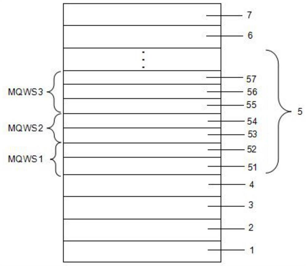
[0048] This embodiment adopts the light-emitting diode chip manufacturing method for improving brightness provided by the present invention, adopts MOCVD to grow GaN-based LED epitaxial wafers, and uses high-purity H 2 or high purity N 2 or high purity H 2 and high purity N 2 The mixed gas as the carrier gas, high-purity NH 3 As the N source, the metal-organic source trimethylgallium (TMGa) is used as the gallium source, trimethylindium (TMIn) is used as the indium source, and the N-type dopant is silane (SiH 4 ), trimethylaluminum (TMAl) as the aluminum source, and the P-type dopant as magnesium dicene (CP 2 Mg), the reaction pressure is between 70mbar and 600mbar. The specific growth method is as follows (for the epitaxial structure, please refer to figure 1 ):

[0049] A method for manufacturing a light-emitting diode chip for improving brightness, which sequentially includes: processing a sapphire substrate 1, growing a low-temperature GaN buffer layer 2, growing a n...

Embodiment 2

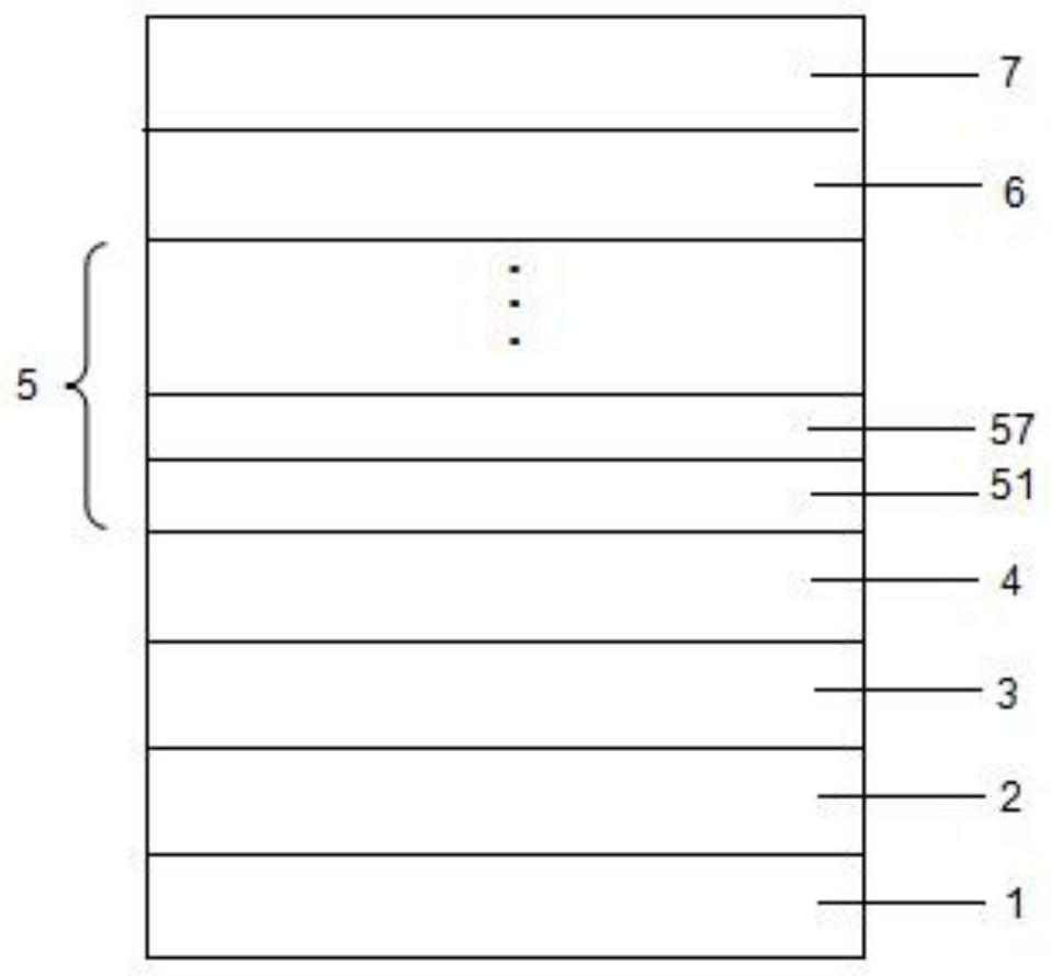
[0085] Comparative examples are provided below, that is, the growth method of the traditional LED epitaxial structure (for the epitaxial structure, please refer to figure 2 ).

[0086] Step 1: At a temperature of 1000-1100°C and a reaction chamber pressure of 100-300mbar, feed 100-130L / min of H 2 Under the conditions, process the sapphire substrate for 5-10 minutes.

[0087] Step 2: growing a low-temperature GaN buffer layer 2 and forming irregular small islands in the low-temperature GaN buffer layer 2 .

[0088] Specifically, the step 2 is further as follows:

[0089] At a temperature of 500-600°C and a reaction chamber pressure of 300-600mbar, 10000-20000sccm of NH is introduced 3 , 50-100sccm TMGa, 100-130L / min H 2 Under the condition of , growing the low-temperature GaN buffer layer 2 on the sapphire substrate 1, the thickness of the low-temperature GaN buffer layer 2 is 20-40nm;

[0090] At a temperature of 1000-1100°C and a reaction chamber pressure of 300-600mbar...


PUM

PropertyMeasurementUnit
thicknessaaaaaaaaaa
thicknessaaaaaaaaaa
thicknessaaaaaaaaaa

Abstract

The invention discloses a light-emitting diode chip manufacturing method capable of improving brightness. The method sequentially comprises the following processes: processing a substrate, growing a low-temperature GaN buffer layer, growing a non-doped GaN layer, growing a Si-doped N-type GaN layer, growing a multi-quantum well layer, growing an AlGaN electron blocking layer, growing a Mg-doped P-type GaN layer, and cooling. The process of growing the multi-quantum well layer sequentially comprises the steps of growing an MQWs1, growing an MQWs2 and growing an MQWs3, the process of growing the MQWs1 comprises the steps of growing an InGaN-1 well layer and an InGaN-2 well layer sequentially, the process of growing the MQWs2 comprises the steps of growing a P-type AlGaN / GaN high-potential barrier structure layer, and the process of growing the MQWs3 comprises the steps of sputtering a SiO2 / Al2O3 thin film and growing a GaN barrier layer. According to the invention, the quality of the quantum well is improved by adopting the novel LED quantum well preparation method, so that the brightness of the LED is improved.

Description

technical field [0001] The invention belongs to the technical field of LEDs, and in particular relates to a method for manufacturing a light-emitting diode chip for improving brightness. Background technique [0002] A light-emitting diode (Light-Emitting Diode, LED) is a semiconductor electronic device that converts electrical energy into light energy. When the LED has current flowing, the electrons and holes in the LED recombine in its multiple quantum wells to emit monochromatic light. As a new type of high-efficiency, environmentally friendly and green solid-state lighting source, LED has the advantages of low voltage, low energy consumption, small size, light weight, long life, high reliability and rich colors. At present, the scale of domestic production of LEDs is gradually expanding, but LEDs still have the problem of low performance, which affects the energy-saving effect of LEDs. [0003] The quality of LED epitaxial InGaN / GaN multiple quantum wells prepared by t...

Claims


Application Information

Patent Timeline
Patent Type & Authority Applications(China)
IPC IPC(8): H01L33/00H01L33/06H01L33/10H01L33/12H01L33/14
CPCH01L33/007H01L33/06H01L33/10H01L33/12H01L33/145
Inventor 徐平
Owner XIANGNENG HUALEI OPTOELECTRONICS
Why Eureka
Try Eureka