10.3-10.9 mum high-strength anti-reflection film on ZnSe substrate and coating method
A 100L1010H901L10H933L10H, anti-reflection coating technology, applied in sputtering coating, vacuum evaporation coating, ion implantation coating and other directions, can solve the problems of high refractive index and scratches of zinc selenide material
- Summary
- Abstract
- Description
- Claims
- Application Information
AI Technical Summary
Problems solved by technology
Method used
Image
Examples
Embodiment 1
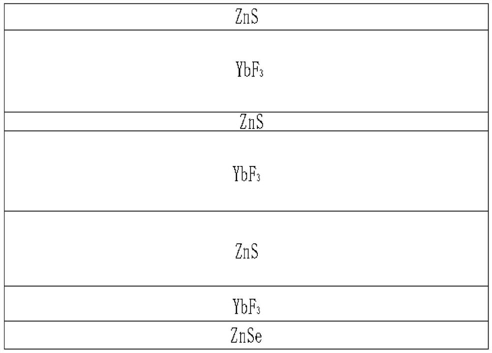
[0034] The substrate is selected from the range of 10.3-10.9 μm, and the APS ion source is used in the ZnSe substrate in Znse base. On the substrate, a 100 nm thickness YBF3 layer is sequentially plated, 1010 nm thickness ZnS layer, 901 nm thickness YBF 3 Layer, 10 nm thickness ZnS layer, 933 nm thickness YBF 3 Layer, 10 nm thickness zns layer. The APS ion source control parameter is the deflection voltage Vb100 ~ 120V, the discharge current Id45 ~ 55mA, the control temperature is 18 ° C to 26 ° C, and the relative humidity is 30% ~ 70%, and the cleanliness is 10,000. ZnS evaporation rate is controlled between 0.6 nm / s, YBF 3 The evaporative rate was controlled between 0.3 nm / s to obtain 10.3-10.9 μm of the ZnSe substrate of the present invention.
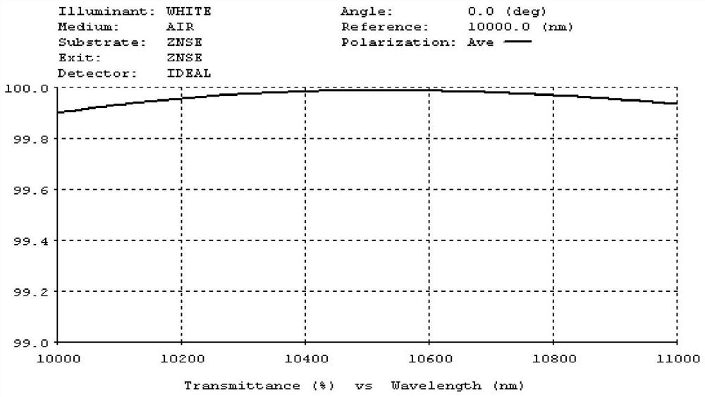
[0035] The resulting ZnSe substrate 10.3-10.9 μm high-strength reduced reaction membrane was measured, and the average transmittance of the reduction of the membrane was 99.50%.
Embodiment 2
[0037] The substrate is selected from the range of 10.3-10.9 μm, and the APS ion source is used in the ZnSe substrate in Znse base. 100 nm thickness is plated in the substrate YBF 3 Layer, 1010 nm thickness ZnS layer, 901 nm thickness YBF 3 Layer, 10 nm thickness ZnS layer, 933 nm thickness YBF 3 Layer, 10 nm thickness zns layer. The APS ion source control parameter is the deflection voltage Vb100 ~ 120V, the discharge current Id45 ~ 55mA, the control temperature is 18 ° C to 26 ° C, and the relative humidity is 30% ~ 70%, and the cleanliness is 10,000. ZnS evaporation rate is controlled between 0.8 nm / s, YBF 3 The evaporative rate was controlled between 0.5 nm / s to obtain a high-strength reduction reaction of the ZNSE substrate of the present invention.
[0038] The obtained ZnSe substrate 10.3-10.9 μm high-strength reduction membrane was measured, and the average transmittance of the reduction of the membrane was 99.70%.
Embodiment 3
[0040]The substrate is selected from the range of 10.3-10.9 μm, and the APS ion source is used in the ZnSe substrate in Znse base. 100 nm thickness is plated in the substrate YBF 3 Layer, 1010 nm thickness ZnS layer, 901 nm thickness YBF 3 Layer, 10 nm thickness ZnS layer, 933 nm thickness YBF3 layer, 10 nm thickness ZnS layer. The APS ion source control parameter is the deflection voltage Vb100 ~ 120V, the discharge current Id45 ~ 55mA, the control temperature is 18 ° C to 26 ° C, and the relative humidity is 30% ~ 70%, and the cleanliness is 10,000. ZnS evaporation rate is controlled between 0.7 nm / s, YBF 3 The evaporation rate was controlled between 0.4 nm / s to obtain a high-strength reduction reaction of the ZnSe substrate of the present invention.
[0041] The resulting ZnSe substrate 10.3-10.9 μm high-strength reduction membrane was measured, and the average transmittance of the reduction of the membrane was 99.60%.
PUM
 Abstract
Description
Claims
Application Information

