High-speed photonic integrated chip based on surface plasmon enhancement and preparation method

A surface plasmon and photon integration technology, applied in the direction of electrical components, final product manufacturing, sustainable manufacturing/processing, etc., can solve the problems of slow response and unadjustable bandwidth, so as to improve the corresponding speed and speed up the current carrying Sub compound rate, effect of improving responsiveness

Active Publication Date: 2021-09-07
NANJING UNIV OF POSTS & TELECOMM
View PDF2 Cites 4 Cited by
  • Summary
  • Abstract
  • Description
  • Claims
  • Application Information

AI Technical Summary

Problems solved by technology

[0006] ZL2009100307856 discloses an integrated optical fiber gyroscope chip based on surface plasmon waveguides, which uses the transmission characteristics of surface plasmon waveguides to realize long-distance transmission of optical signals with single polarization, and directly modulates the core layer of surface plasmon waveguides. And there is a specific structure to eliminate the influence of light leakage on the accuracy of the fiber optic gyroscope, but its bandwidth cannot be adjusted and its response is slow

Method used


Image

  • High-speed photonic integrated chip based on surface plasmon enhancement and preparation method
  • High-speed photonic integrated chip based on surface plasmon enhancement and preparation method
  • High-speed photonic integrated chip based on surface plasmon enhancement and preparation method

Examples


Embodiment Construction

[0042] Embodiments of the present invention will be disclosed in the following diagrams. For the sake of clarity, many practical details will be described together in the following description. It should be understood, however, that these practical details should not be used to limit the invention. That is, in some embodiments of the invention, these practical details are not necessary.

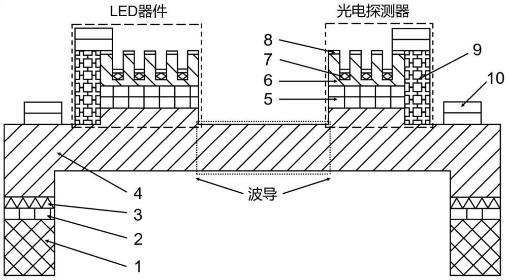
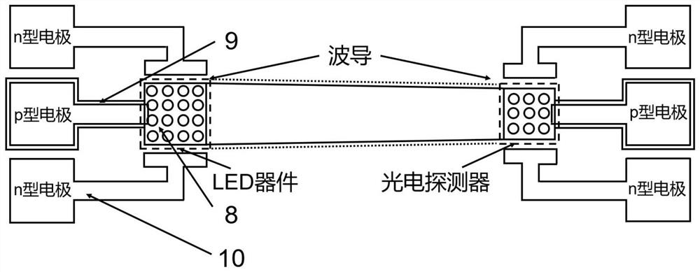
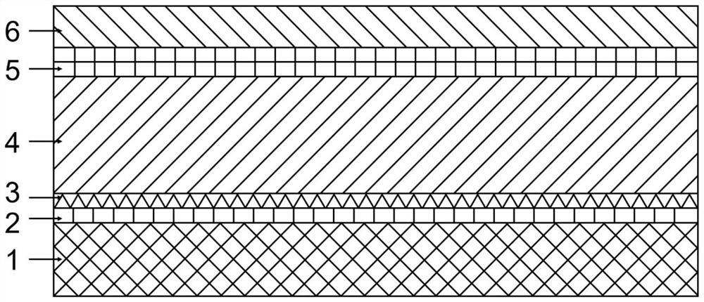
[0043] Such as Figure 1-2 As shown, the present invention is a high-speed photonic integrated chip based on surface plasmon enhancement, with InGaN / GaN multi-quantum well LED epitaxial wafers as the carrier, including a silicon substrate layer 1, a buffer layer arranged on the silicon substrate layer 1 2. The non-doped GaN layer 3 disposed on the buffer layer 2, the n-type GaN layer 4 disposed on the non-doped GaN layer 3, the InGaN / GaN multiple quantum well layer 5 disposed on the n-type GaN layer 4, and the The p-type GaN layer 6 on the InGaN / GaN multi-quantum well layer 5; the LED devic...


PUM

PropertyMeasurementUnit
depthaaaaaaaaaa
thicknessaaaaaaaaaa
thicknessaaaaaaaaaa

Abstract

The invention relates to a high-speed photon integrated chip based on surface plasmon enhancement and a preparation method. The chip takes a silicon substrate LED epitaxial wafer as a carrier, an LED device and a photoelectric detector are arranged on the silicon substrate LED epitaxial wafer, the LED device and the photoelectric detector are connected through a waveguide, and the LED device and the photoelectric detector each comprise a p-n junction, a p-type electrode and an n-type electrode. The surface plasmon enhanced LED device, the optical waveguide and the surface plasmon enhanced photoelectric detector are integrated on the same chip, and light emitted by the LED device is laterally coupled into the optical waveguide, is transmitted through the optical waveguide and is detected by the photoelectric detector at the other end of the waveguide. The surface plasmon coupling effect can improve the modulation bandwidth of the LED device and the responsivity of the photoelectric detector, and meanwhile, increase the overlapping degree of the light-emitting spectrum of the LED and the response spectrum of the detector, and finally a high-speed photon integrated chip is achieved.

Description

technical field [0001] The invention relates to the field of semiconductor optoelectronic devices and integration, in particular to a high-speed photonic integrated chip based on surface plasmon enhancement and a preparation method. Background technique [0002] Visible light communication technology is a new type of wireless optical transmission technology that uses visible light for data communication. Compared with traditional wireless communication technology, visible light communication technology has the advantages of high bandwidth, strong anti-interference, good confidentiality, and no electromagnetic radiation. With the rapid development and popularization of light-emitting diodes, the increasing demand for high-speed wireless access, and the pull of the future 6G layout, visible light communication technology has developed rapidly in recent years. Gallium nitride (GaN)-based materials have excellent optical and electrical properties, and can realize a homogeneous p...

Claims


Application Information

Patent Timeline
Patent Type & Authority Applications(China)
IPC IPC(8): H01L31/173H01L31/0352H01L31/18
CPCH01L31/173H01L31/035236H01L31/1848H01L31/1852Y02P70/50
Inventor 张国刚王永进
Owner NANJING UNIV OF POSTS & TELECOMM
Why Eureka
Try Eureka