HKMG structure manufacturing method
A manufacturing method and metal gate technology, applied in the manufacture of semiconductor/solid-state devices, electrical components, transistors, etc., can solve the problems of Al filling defects in metal gates, affecting the performance of semiconductor devices, aluminum diffusion, etc.
- Summary
- Abstract
- Description
- Claims
- Application Information
AI Technical Summary
Problems solved by technology
Method used
Image

Examples
no. 1 example ;
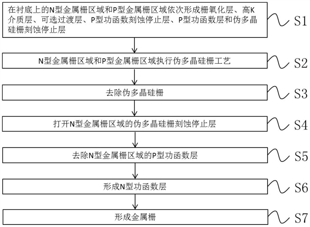
[0032] Such as figure 1 As shown, the HKMG structure fabrication method provided by the present invention comprises the following steps:
[0033] S1, in the N-type metal gate region and the P-type metal gate region on the substrate, a gate oxide layer, a high-K dielectric layer, an optional transition layer, a P-type work function etch stop layer, a P-type work function layer and a dummy polysilicon gate etch stop layer;
[0034] S2, performing a dummy polysilicon gate process on the N-type metal gate region and the P-type metal gate region;
[0035] S3, removing the dummy polysilicon gate;
[0036] S4, opening the dummy polysilicon gate etch stop layer in the N-type metal gate region;
[0037] S5, removing the P-type work function layer in the N-type metal gate region;
[0038] S6, forming an N-type work function layer;
[0039] S7, forming a metal grid.
[0040] In addition, it should also be understood that although the terms "first", "second", etc. may be used herein...
no. 2 example ;
[0042] continue to refer figure 1 As shown, the HKMG structure fabrication method provided by the present invention comprises the following steps:
[0043] S1, in the N-type metal gate region and the P-type metal gate region on the substrate, a gate oxide layer, a high-K dielectric layer, an optional transition layer, a P-type work function etch stop layer, a P-type work function layer and a dummy polysilicon gate etch stop layer;
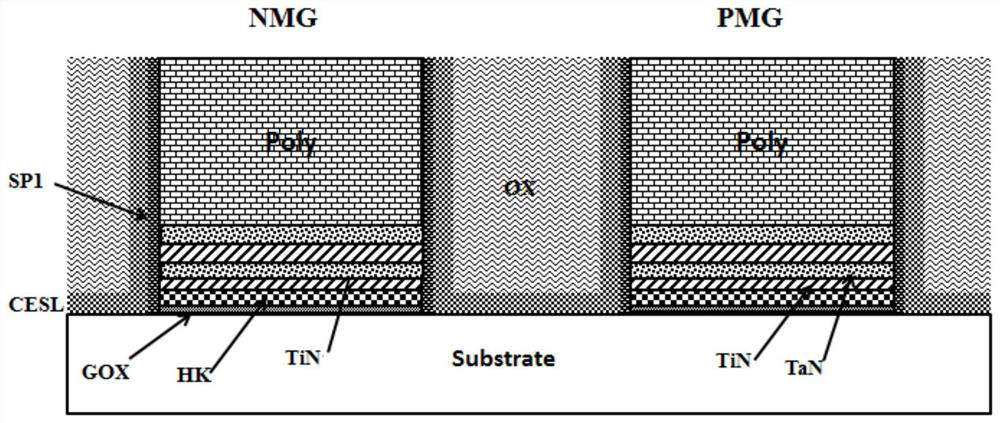
[0044] S2, such as figure 2 As shown, the N-type metal gate region and the P-type metal gate region perform a dummy polysilicon gate process;
[0045] S3, removing the dummy polysilicon gate;
[0046] S4, opening the dummy polysilicon gate etch stop layer in the N-type metal gate region;
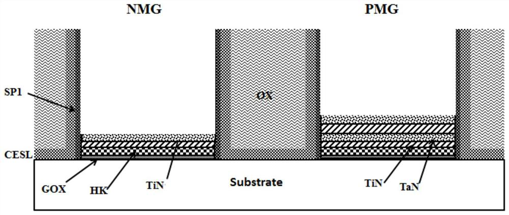
[0047] S5, such as image 3 As shown, the P-type work function layer in the N-type metal gate region is removed by a wet etching process;
[0048] S6, forming an N-type work function layer;
[0049] S7, forming a metal grid.
[0050] Wherein, the P-type wo...
PUM
 Abstract
Description
Claims
Application Information
PatSnap Eureka turns technology decisions into work you can execute. Powered by our Innovation Knowledge Graph, it runs expert workflows across engineering, life sciences, materials and intellectual property. Get your review-ready output in minutes.


