A radiation-hardened sic device structure based on distributed capacitance

A radiation hardening, device structure technology, applied in electrical components, semiconductor devices, circuits, etc., can solve problems such as catastrophic accidents, failures, and inability to meet the requirements of aerospace applications in electronic systems, and achieve the effect of improving the ability to resist single particles

Active Publication Date: 2022-05-20
FUDAN UNIV
View PDF0 Cites 0 Cited by
  • Summary
  • Abstract
  • Description
  • Claims
  • Application Information

AI Technical Summary

Problems solved by technology

Due to its special single event effect relative to Si-based power devices, the current commercial SiC devices cannot meet the requirements of aerospace, which can cause violent fluctuations or even complete failure of the power supply, resulting in catastrophic accidents in satellite electronic systems, which cannot meet aerospace applications. Require

Method used


Image

  • A radiation-hardened sic device structure based on distributed capacitance
  • A radiation-hardened sic device structure based on distributed capacitance
  • A radiation-hardened sic device structure based on distributed capacitance

Examples


Embodiment 1

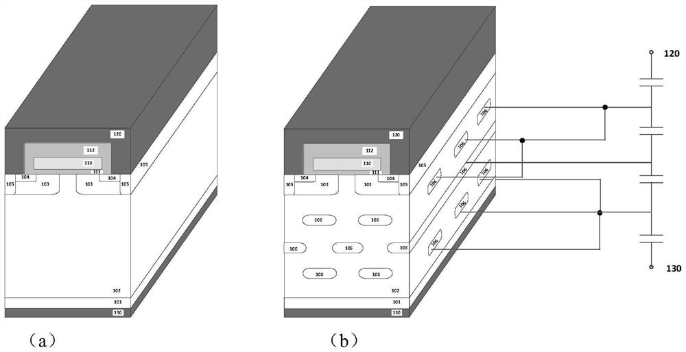
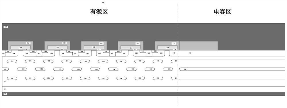
[0019] Taking the MOSFET device as an example, the basic structure of the present invention is compared with the traditional structure such as figure 1 . The main structure Including, a SiC substrate 101 of the first doping type, a SiC epitaxial layer 102 of the first doping type grown on the substrate, a well 103 of the second doping type implanted in the epitaxial layer, and implanted in the well Formed first doping type source 104, second doping type ohmic contact region 105, gate oxide layer 111, metal or polycrystalline gate 110, isolation dielectric layer 112, and metal source on the SiC epitaxial surface 120, and the metal drain 130 will be connected to the bottom. There is no essential difference in appearance between the above structure and the traditional MOSFET, but the only difference lies in the highly doped region 106 of the second doping type distributed in the low doping epitaxial layer 102 of the first doping type. The above two doping types can be interch...


PUM


Abstract

The invention discloses a radiation-strengthened SiC device structure based on distributed capacitance; the invention interleaves distributed floating high-doping-concentration epitaxial layers in the active region's low-doping-concentration first-doping-type epitaxial layer The second doping type structure, the second doping type structure of the same layer with the same vertical position and high doping concentration is arranged at intervals of several active region cells; the first doping region with low doping concentration and high doping concentration between layers The alternating composite structure of the second doped region of the doping concentration forms a PN alternating capacitance, which is arranged vertically from the top electrode to the bottom electrode, and is respectively connected to the floating PN of the same layer in the non-active region for storing charges. junction capacitance connection. The present invention limits the local electric field when a single particle is input through the voltage stabilizing effect formed by the distributed capacitance of multiple series PN junctions, and shunts the local current on the single particle path to "temporarily store it at the distributed capacitance", thereby limiting the device localized power to prevent overheating.

Description

technical field [0001] The invention belongs to the technical field of integrated circuits, and in particular relates to a radiation-hardened SiC device structure based on distributed capacitance. Background technique [0002] Silicon carbide SBD (Schottky diode), JFET (junction field effect transistor), MOSFET (metal oxide field effect transistor) and other device technologies have gradually matured. Penetration, and in the field of military industry, it is also applied in fields such as propulsion and radar power supply. However, in the field of aerospace, its radiation effects under various particles, ions, and rays in space and reinforcement technology have been widely concerned. Due to its special single event effect relative to Si-based power devices, the current commercial SiC devices cannot meet the requirements of aerospace, which can cause violent fluctuations or even complete failure of the power supply, resulting in catastrophic accidents in satellite electronic...

Claims


Application Information

Patent Timeline
Patent Type & Authority Patents(China)
IPC IPC(8): H01L29/06H01L29/78
CPCH01L29/7827H01L29/0684H01L29/0696H01L29/7802H01L29/0623H01L29/1608
Inventor 孙博韬张清纯
Owner FUDAN UNIV
Why Eureka
Try Eureka