Growth method of beta-Ga2O3 film

A growth method, -ga2o3 technology, applied in the field of semiconductor thin film growth, can solve the problems of high surface roughness and multiple dislocations in thin films, and achieve the effect of reducing surface roughness, realizing transition, and enhancing two-dimensional growth.

Pending Publication Date: 2021-10-29
XIDIAN UNIV
View PDF0 Cites 0 Cited by
  • Summary
  • Abstract
  • Description
  • Claims
  • Application Information

AI Technical Summary

Problems solved by technology

About β-Ga 2 o 3 The heteroepitaxy of thin films is mainly concentrated on the sapphire substrate, but the β-Ga obtained by epitaxy 2 o 3 Thin films have more dislocations and higher surface roughness, which makes it difficult to apply in electronic devices

Method used


Image

  • Growth method of beta-Ga2O3 film
  • Growth method of beta-Ga2O3 film

Examples


Embodiment 1

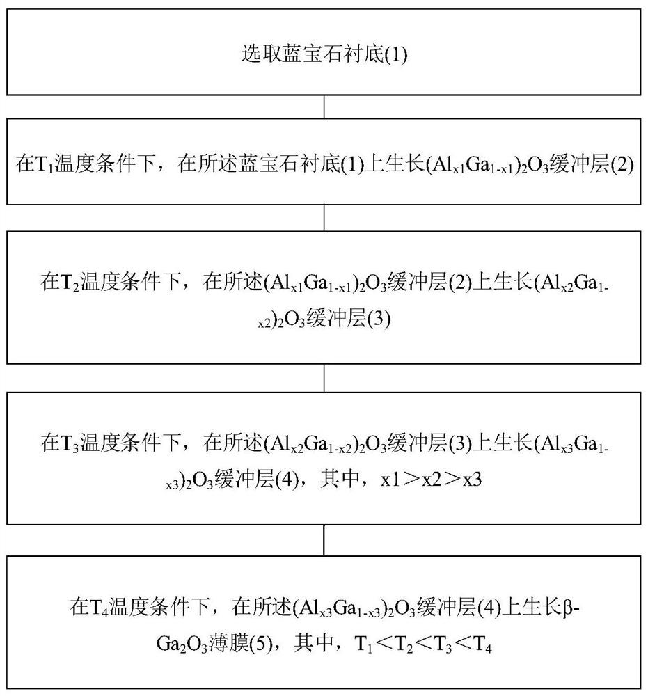
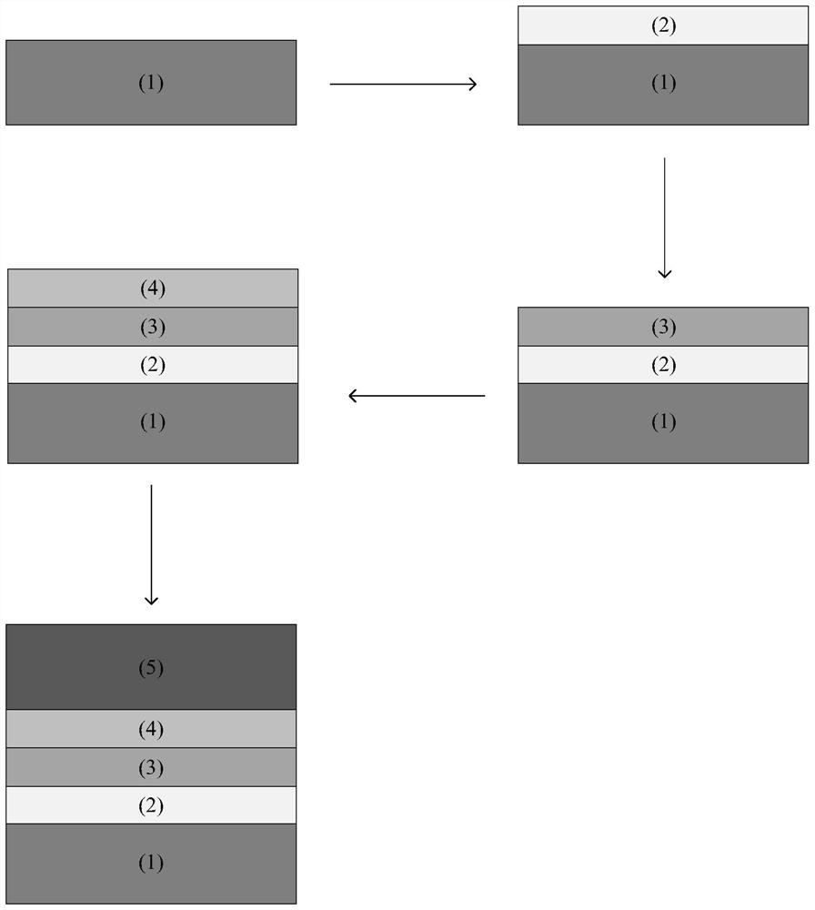
[0036] See figure 1 , figure 2 , figure 1 One β-Ga provided by the embodiment of the present invention 2 O 3 A flow chart of the growth method of the film, figure 2 One β-Ga provided by the embodiment of the present invention 2 O 3 A process diagram of the preparation of the growth method of the film. The present invention provides a β-Ga 2 O 3 The growth method of the film, the growth method includes the following steps:

[0037] Step 1, select the sapphire substrate 1.

[0038] Specifically, the sapphire substrate is placed in an HF acid solution for soaking, then the sapphire substrate is soaked with alcohol and acetone, then rinse the sapphire substrate after the flowing deionized water, and finally blows with high purity nitrogen. The sapphire substrate after drying.

[0039] Preferably, the HF acid solution consists of a solution having a HF acid content of 30%.

[0040] Preferably, the sapphire substrate 1 includes a chemically mechanical polished C-Plane sapphire substrate...

Embodiment 2

[0068] The present embodiment provides a production of 3 min (Al) based on the above embodiment 1-x GA x ) 2 O 3 Buffer β-Ga 2 O 3 Growth method of film.

[0069] Step 1, the sapphire substrate was submerged in a solution of the HF acid content of 30%, and then washed with alcohol and acetone, then rinsed with a flow of deionized water, and finally was blown with high purity nitrogen.

[0070] Step 2, epitaxial growth 3 min (Al 0.8 GA 0.2 ) 2 O 3 buffer layer.

[0071] Specifically, the cleaning sapphire substrate is placed in a low pressure MOCVD reaction chamber, high purity O 2 For the O source, the temperature of the reaction chamber is 500 ° C in TEGA and TEAL, respectively, and the growth pressure is 40 torr, TEGA flow is 40 sccm, and TEAL flow is 40sccm, O 2 The flow rate is 2100 sccm, and the growth of 3 min is extends on sapphire substrate (Al 0.8 GA 0.2 ) 2 O 3 buffer layer.

[0072] Step 3 and improve the growth temperature.

[0073] Specifically, maintaining other grow...


PUM

PropertyMeasurementUnit
thicknessaaaaaaaaaa

Abstract

The invention relates to a growth method of a beta-Ga2O3 film. The growth method comprises the following steps of selecting a sapphire substrate; growing a (Alx1Ga1-x1)2O3 buffer layer on the sapphire substrate under a T1 temperature condition; under a T2 temperature condition, growing a (Alx2Ga1-x2)2O3 buffer layer on the (Alx1Ga1-x1)2O3 buffer layer; under a T3 temperature condition, growing a (Alx3Ga1-x3)2O3 buffer layer on the (Alx2Ga1-x2)2O3 buffer layer, wherein x1> x2> x3; and under a T4 temperature condition, growing the beta-Ga2O3 film grows on the (Alx3Ga1-x3)2O3 buffer layer , and T1<T2<T3<T4. According to the invention, the (Al1-xGax) 2O3 buffer layer growing at variable temperature is introduced between the beta-Ga2O3 film and the sapphire substrate, and the introduction of the (Al1-xGax) 2O3 buffer layer not only realizes the uniform transition of element components between the substrate and the film, but also realizes the transition of a lattice structure, so that the dislocation caused by the lattice mismatch is reduced. According to different element components among the buffer layers, different growth temperatures are adopted, so that the growth quality of the buffer layers is improved, the two-dimensional growth of the beta-Ga2O3 film is enhanced, and the surface roughness of the film is reduced.

Description

Technical field [0001] The invention belongs to the semiconductor film growth technology, involving a β-Ga 2 O 3 Growth method of film. Background technique [0002] With the improvement of semiconductor device performance requirements, traditional SI base devices are gradually facing many challenges, and their lower breakdown voltage is increasingly difficult to apply in high-power high-power devices. β-Ga 2 O 3 As the third-generation semiconductor material has a banned bandwidth of up to 5EV, it makes it breakdown voltage and breakdown electric field far more than Si material, and its Balea is also greater than the third-generation semiconductor material such as GaN, Therefore, β-Ga 2 O 3 It has great potential in the application of electronic devices. [0003] GA 2 O 3 The semiconductor material has 5 different structures, namely α-, β-, γ-, δ-, ε-. The most stable and most application is β-Ga 2 O 3 . About β-Ga 2 O 3 The heterogeneous epitaxial of the film is mainly concentr...

Claims


Application Information

Patent Timeline
Patent Type & Authority Applications(China)
IPC IPC(8): H01L21/02
CPCH01L21/02565H01L21/02483H01L21/02609H01L21/0237H01L21/0262
Inventor 张涛冯倩张雅超张进成马佩军郝跃
Owner XIDIAN UNIV
Why Eureka
Try Eureka