Homoepitaxial beta-Ga2O3 film and preparation method thereof

A homoepitaxial, -ga2o3 technology, applied in the field of microelectronics, can solve problems such as rough surface morphology, device leakage, and reduce carrier mobility, and achieve enhanced two-dimensional growth, improved device performance, and reduced dislocation density. Effect

Pending Publication Date: 2021-10-19
XIDIAN UNIV
View PDF6 Cites 0 Cited by
  • Summary
  • Abstract
  • Description
  • Claims
  • Application Information

AI Technical Summary

Problems solved by technology

[0003] Currently, due to β-Ga 2 o 3 The homoepitaxy of thin films has always been a difficult subject, and it is also difficult to achieve two-dimensional growth of thin films on homogeneous substrates with poor quality, which leads to the fact that the existing homoepitaxial β-Ga 2 o 3 The epitaxial film still has a large density of dislocations and a relatively rough surface morphology, and the high surface roughness of the film will affect the contact between the metal electrode and the film, thereby causing device leakage; at the same time, the more boundaries on the film surface also limit the load capacity. The transport of carriers reduces the mobility of carriers, which in turn limits the application of thin film materials in devices

Method used


Image

  • Homoepitaxial beta-Ga2O3 film and preparation method thereof
  • Homoepitaxial beta-Ga2O3 film and preparation method thereof
  • Homoepitaxial beta-Ga2O3 film and preparation method thereof

Examples


Embodiment 1

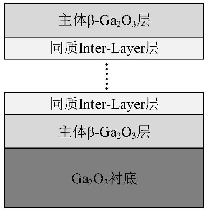
[0036] See figure 1 , figure 1 It is a kind of homoepitaxial β-Ga provided by the embodiment of the present invention 2 o 3 Schematic diagram of the structure of thin films, including Ga 2 o 3 substrate and located at Ga 2 o 3Layered β-Ga on a substrate 2 o 3 structure, where layered β-Ga 2 o 3 The structure consists of several spaced apart host β-Ga 2 o 3 layer and homogeneous Inter-Layer layer, and layered β-Ga 2 o 3 The top and bottom layers of the structure are host β-Ga 2 o 3 layer; the grain size of each homogeneous Inter-Layer layer is the same as that of two adjacent host β-Ga 2 o 3 The layers differ in grain size.

[0037] In this embodiment, the homogeneous Inter-Layer layer and the host β-Ga 2 o 3 The material of the layers is the same, that is, β-Ga 2 o 3 Inter-Layer layer.

[0038] Further, the host β-Ga 2 o 3 The thickness of the layer is greater than that of the homogeneous Inter-Layer layer.

[0039] Theoretically, the thicker the homog...

Embodiment 2

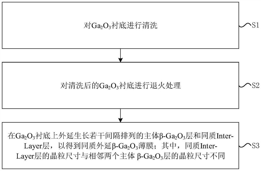
[0045] On the basis of the first embodiment above, this embodiment provides a homoepitaxial β-Ga 2 o 3 The method of film preparation. See image 3 , image 3 It is a kind of homoepitaxial β-Ga provided by the embodiment of the present invention 2 o 3 Schematic diagram of the preparation method of the film, specifically comprising the following steps:

[0046] S1: for Ga 2 o 3 The substrate is cleaned.

[0047] In this embodiment, the RCA standard cleaning method is used to clean the β-Ga 2 o 3 The substrate is cleaned. Specifically include:

[0048] S11: to β-Ga 2 o 3 The substrates were sequentially cleaned with organic and deionized water.

[0049] First, for Ga 2 o 3 The substrate is polished, and then the polished Ga 2 o 3 The substrate is cleaned in an organic cleaning solution at 60-80°C for 15-20 minutes to remove organic contamination on the substrate surface; finally, the organic-cleaned substrate is cleaned with flowing deionized water for 40-60 se...

Embodiment 3

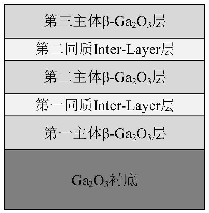
[0071] On the basis of the second embodiment above, this embodiment grows three layers of main body β-Ga 2 o 3 layer and two Inter-Layer layers as examples, the specific preparation process of the present invention will be described in detail. See Figures 4a-4f , Figures 4a-4f It is a kind of homoepitaxial β-Ga provided by the embodiment of the present invention 2 o 3 Schematic diagram of the preparation process of the film, specifically including:

[0072] Step 1: Select single crystal β-Ga 2 o 3 As a substrate material, such as Figure 4a As shown, it is then polished and standardized to clean; this includes:

[0073] 1a) The polished Ga 2 o 3 The substrate is cleaned in an organic cleaning solution at 80°C for 20 minutes;

[0074] 1b) Cleaning the organically cleaned substrate with flowing deionized water for 40 seconds;

[0075] 1c) putting the cleaned substrate into a solution with HF content of 30% and corroding for 60s;

[0076] 1d) The etched β-Ga 2 o ...


PUM


Abstract

The invention discloses a homoepitaxial beta-Ga2O3 film and a preparation method thereof. The film comprises a Ga2O3 substrate and a layered beta-Ga2O3 structure located on the Ga2O3 substrate; the layered beta-Ga2O3 structure comprises a plurality of main body beta-Ga2O3 layers and homogeneous Inter-Layer layers which are arranged at intervals; the top layer and the bottom layer of the layered beta-Ga2O3 structure are the main body beta-Ga2O3 layers; the grain size of each homogeneous Inter-Layer layer is different from the grain sizes of the two adjacent main body beta-Ga2O3 layers. The homogeneous Inyer-Layer layers are introduced into a traditional homogeneous epitaxial beta-Ga2O3 film structure to form a layered structure with the main body beta-Ga2O3 layers, and the homogeneous Inyer-Layer layers and the main body beta-Ga2O3 layers have different crystal grain sizes, so that crystal grains of the homogeneous Inyer-Layer layers and the main body beta-Ga2O3 layers can be embedded with each other, on one hand, dislocation growth is blocked, the dislocation density in the film is reduced, on the other hand, the two-dimensional growth of the film is enhanced, the flatness of the film is improved, and the performance of the device is improved.

Description

technical field [0001] The invention belongs to the technical field of microelectronics, in particular to a homoepitaxial β-Ga 2 o 3 Thin films and methods for their preparation. Background technique [0002] With the development of microelectronics technology, the wide application of high-breakdown and high-power devices has gradually encountered more challenges to traditional silicon-based and other narrow-bandgap semiconductor materials. Therefore, breakdown voltage has gradually become one of the key factors to measure device performance. . As a third-generation semiconductor material, β-Ga 2 o 3 The forbidden band width is about 5eV, and the breakdown field strength is equivalent to more than 2 times that of SiC and GaN. β-Ga 2 o 3 The Ballyga figure of merit of β-Ga is also much larger than that of Si material, so β-Ga 2 o 3 Thin films have great potential in the application of high-power high-breakdown devices and solar-blind detectors. [0003] Currently, d...

Claims


Application Information

Patent Timeline
Patent Type & Authority Applications(China)
IPC IPC(8): H01L21/02
CPCH01L21/02414H01L21/02565H01L21/02587H01L21/02609H01L21/0262
Inventor 张涛冯倩张雅超张进成马佩军郝跃
Owner XIDIAN UNIV
Why Eureka
Try Eureka