Silicon carbide power semiconductor device and field effect transistor

A power semiconductor, silicon carbide technology, applied in semiconductor devices, electrical components, circuits, etc., can solve problems such as large switching losses

Active Publication Date: 2021-10-29
SONGSHAN LAKE MATERIALS LAB +1
View PDF10 Cites 0 Cited by
  • Summary
  • Abstract
  • Description
  • Claims
  • Application Information

AI Technical Summary

Problems solved by technology

However, the switching loss of existin

Method used


Image

  • Silicon carbide power semiconductor device and field effect transistor
  • Silicon carbide power semiconductor device and field effect transistor
  • Silicon carbide power semiconductor device and field effect transistor

Examples


Embodiment Construction

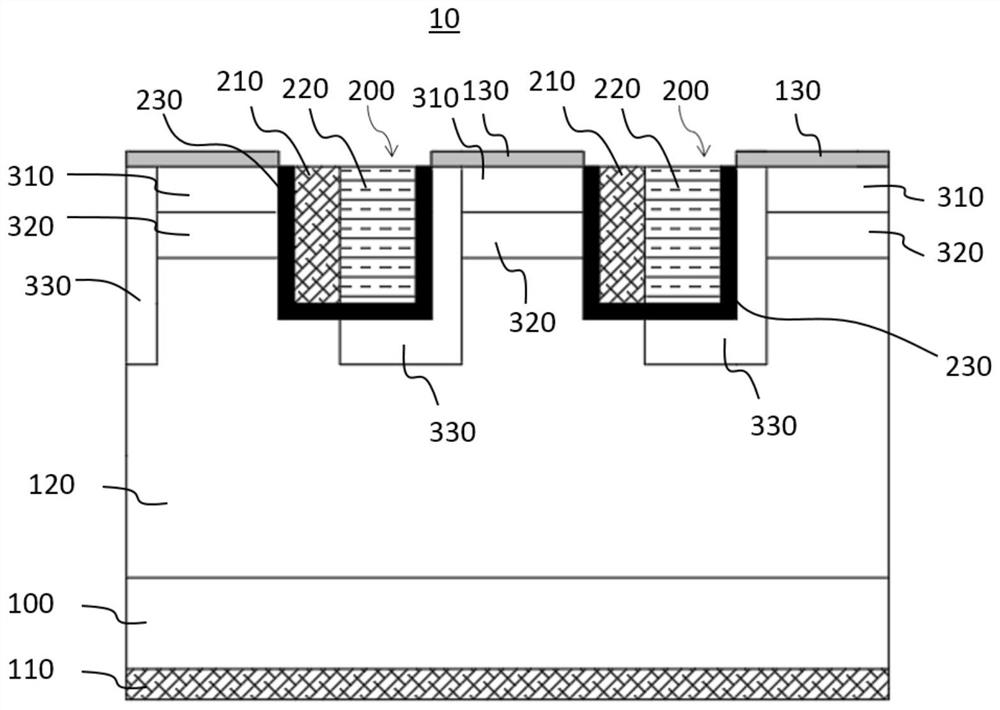
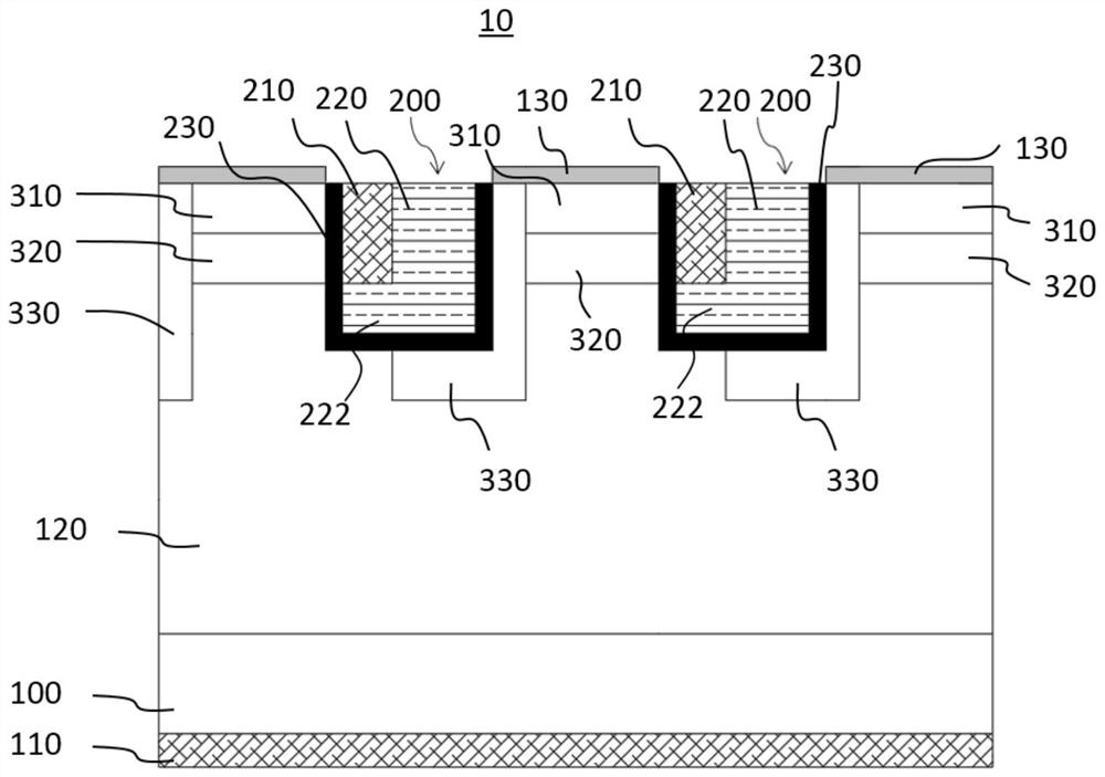
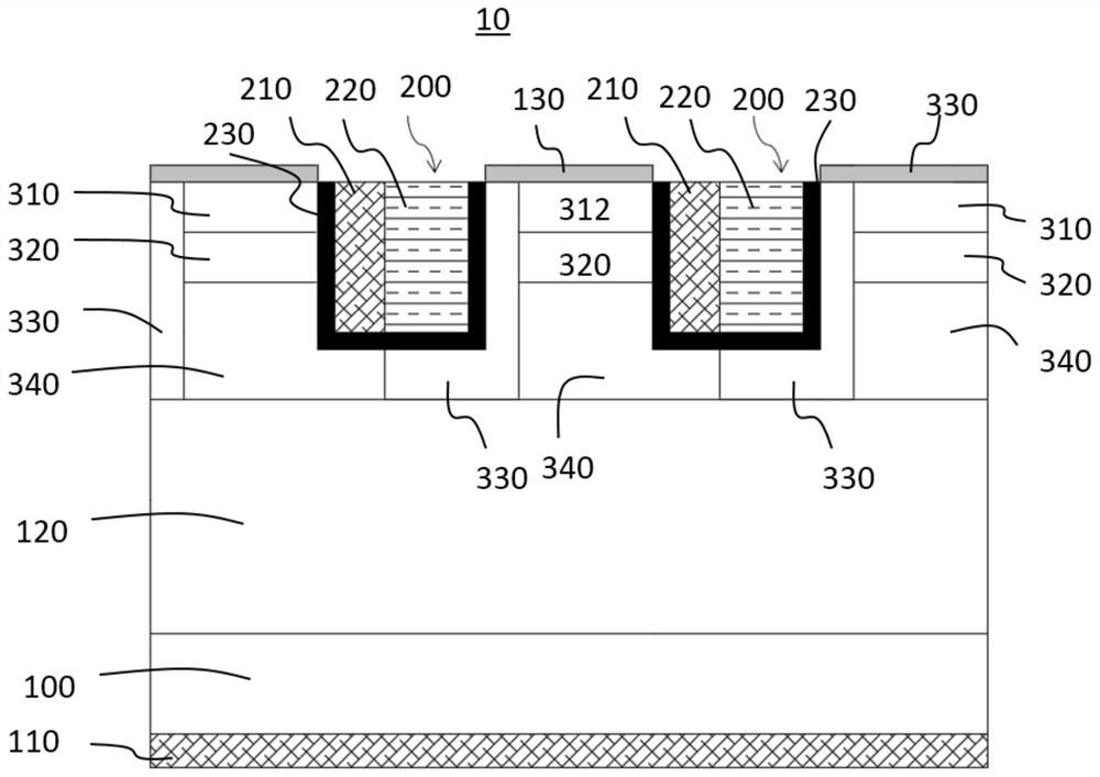
[0025] In order to facilitate the understanding of the present application, the present application will be described more fully below with reference to the relevant drawings. Embodiments of the application are given in the drawings. However, the present application can be embodied in many different forms and is not limited to the embodiments described herein. On the contrary, the purpose of providing these embodiments is to make the disclosure of this application more thorough and comprehensive.

[0026] Unless otherwise defined, all technical and scientific terms used herein have the same meaning as commonly understood by one of ordinary skill in the technical field to which this application belongs. The terms used herein in the specification of the application are only for the purpose of describing specific embodiments, and are not intended to limit the application.

[0027] It will be understood that when an element or layer is referred to as being "on," "adjacent," "con...


PUM

PropertyMeasurementUnit
Widthaaaaaaaaaa
Widthaaaaaaaaaa
Thicknessaaaaaaaaaa

Abstract

The invention relates to a silicon carbide power semiconductor device and a field effect transistor. The silicon carbide power semiconductor device comprises a substrate and a plurality of grid electrode grooves arranged at intervals, the plurality of spaced grid electrode grooves are formed at one side of the substrate, and a first grid electrode and a second grid electrode are arranged in each grid electrode groove. The first grid electrode and the second grid electrode are arranged along the extending direction of the substrate, the first grid electrode is of a first conductivity type. and the second grid electrode is of a second conductive type. A grid electrode oxide layer is formed on the inner wall of each grid electrode groove, and is located between the inner wall of the grid electrode groove and the first grid electrode and the second grid electrode. After the first grid electrode and the second grid electrode form a PN junction, the second grid electrode is completely exhausted by the first grid electrode, and a space charge region is formed. The space charge region can bear voltage, equivalently, the thickness of the grid electrode oxide layer is increased, and with the increase of the thickness of the grid electrode oxide layer, the capacitance between the grid electrode and a shielding region is reduced, so that the grid charge is further reduced, the switching rate can be improved, and the switching loss is reduced.

Description

technical field [0001] The present application relates to the field of semiconductors, in particular to a silicon carbide power semiconductor device and a field effect transistor. Background technique [0002] The third-generation semiconductor silicon carbide (SiC) and gallium nitride (GaN) are wide-bandgap semiconductor materials, which have the advantages of high breakdown electric field strength, good thermal stability, and high carrier saturation drift speed. They are used in high-power devices. Application advantages. Power semiconductor devices are often used in high-voltage, high-current, and high-temperature working environments, and have gradually replaced traditional silicon (Si) materials in the field of power electronics. However, the switching loss of existing power semiconductor devices is relatively large. Contents of the invention [0003] Based on this, it is necessary to provide a silicon carbide power semiconductor device and a field effect transistor...

Claims


Application Information

Patent Timeline
IPC IPC(8): H01L29/423H01L29/06H01L29/739H01L29/78
CPCH01L29/7827H01L29/7398H01L29/7397H01L29/4236H01L29/42364H01L29/0611
Inventor 陈昭铭张安平刘鸣然袁朝城殷鸿杰罗惠馨
Owner SONGSHAN LAKE MATERIALS LAB
Why Eureka
Try Eureka