Single-wavelength and dual-wavelength switchable semiconductor laser and preparation method thereof
A technology of semiconductors and lasers, which is applied in the field of single- and double-wavelength switchable semiconductor lasers and their preparation. It can solve the problems of not being able to emit lasers with a single wavelength, and achieve high integration and simple manufacturing processes.
- Summary
- Abstract
- Description
- Claims
- Application Information
AI Technical Summary
Problems solved by technology
Method used
Image

Examples
Embodiment Construction
[0031] Hereinafter, embodiments of the present invention will be described with reference to the accompanying drawings. In the following description, the same blocks are denoted by the same reference numerals. With the same reference numerals, their names and functions are also the same. Therefore, its detailed description will not be repeated.
[0032] In order to make the object, technical solution and advantages of the present invention clearer, the present invention will be further described in detail below in conjunction with the accompanying drawings and specific embodiments. It should be understood that the specific embodiments described here are only used to explain the present invention, but not to limit the present invention.
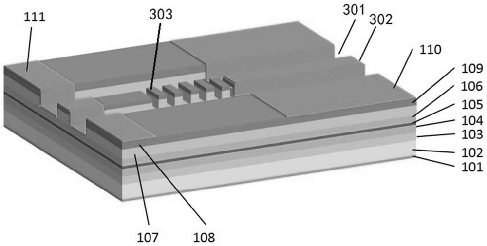
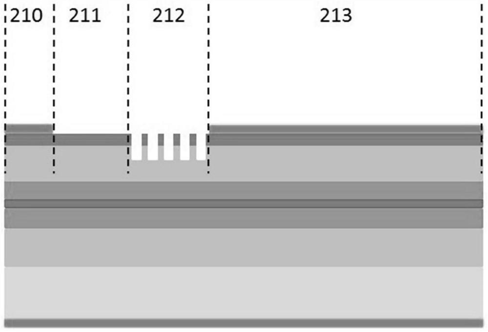
[0033] figure 1 and figure 2 The three-dimensional structure and the cross-sectional structure of the single-wavelength and dual-wavelength switchable semiconductor laser provided by the embodiment of the present invention.
[0034] Such...
PUM
| Property | Measurement | Unit |
|---|---|---|
| Doping concentration | aaaaa | aaaaa |
| Cavity length | aaaaa | aaaaa |
| Width | aaaaa | aaaaa |
Abstract
Description
Claims
Application Information
 - R&D
- Intellectual Property
- Life Sciences
- Materials
- Tech Scout
- Unparalleled Data Quality
- Higher Quality Content
- 60% Fewer Hallucinations
Browse by: Latest US Patents, China's latest patents, Technical Efficacy Thesaurus, Application Domain, Technology Topic, Popular Technical Reports.
© 2025 PatSnap. All rights reserved.Legal|Privacy policy|Modern Slavery Act Transparency Statement|Sitemap|About US| Contact US: help@patsnap.com