
Antimony-based photocathode Sb2S3/Sb2O3 heterojunction structure and preparation method thereof

A heterojunction, antimony-based optical technology, applied in final product manufacturing, sustainable manufacturing/processing, electrical components, etc., can solve photogenerated carrier separation and transmission speed limitations, reduce carrier separation efficiency, and limit energy Conversion efficiency and other issues, to achieve good electronic conductivity, good co-solubility, and improve charge transfer efficiency and stability.

Pending Publication Date: 2021-11-19
KUNMING UNIV OF SCI & TECH
View PDF2 Cites 0 Cited by
  • Summary
  • Abstract
  • Description
  • Claims
  • Application Information

AI Technical Summary

Problems solved by technology

However, Sb 2 o 3 The bandgap width is 3.0eV, and only about 5% of the total solar energy can be absorbed and utilized, which limits the improvement of its energy conversion efficiency. Separation and transport speeds are limited, which reduces carrier separation efficiency, which in turn limits energy conversion efficiency improvements

Method used


Image

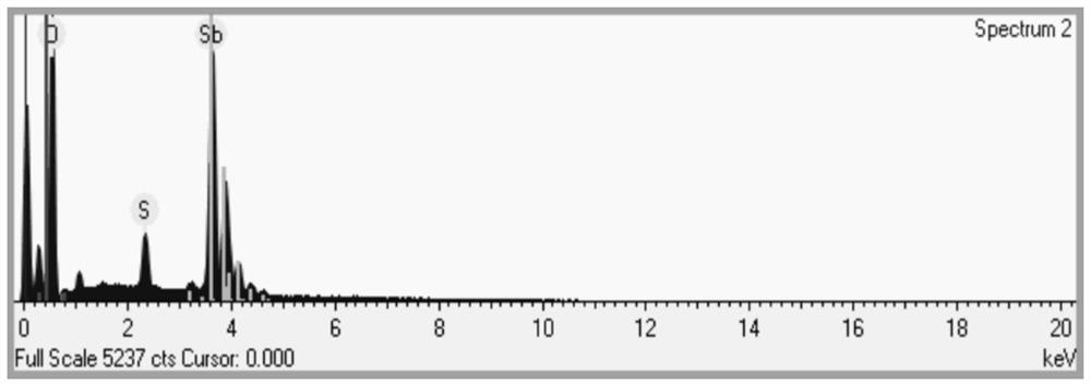
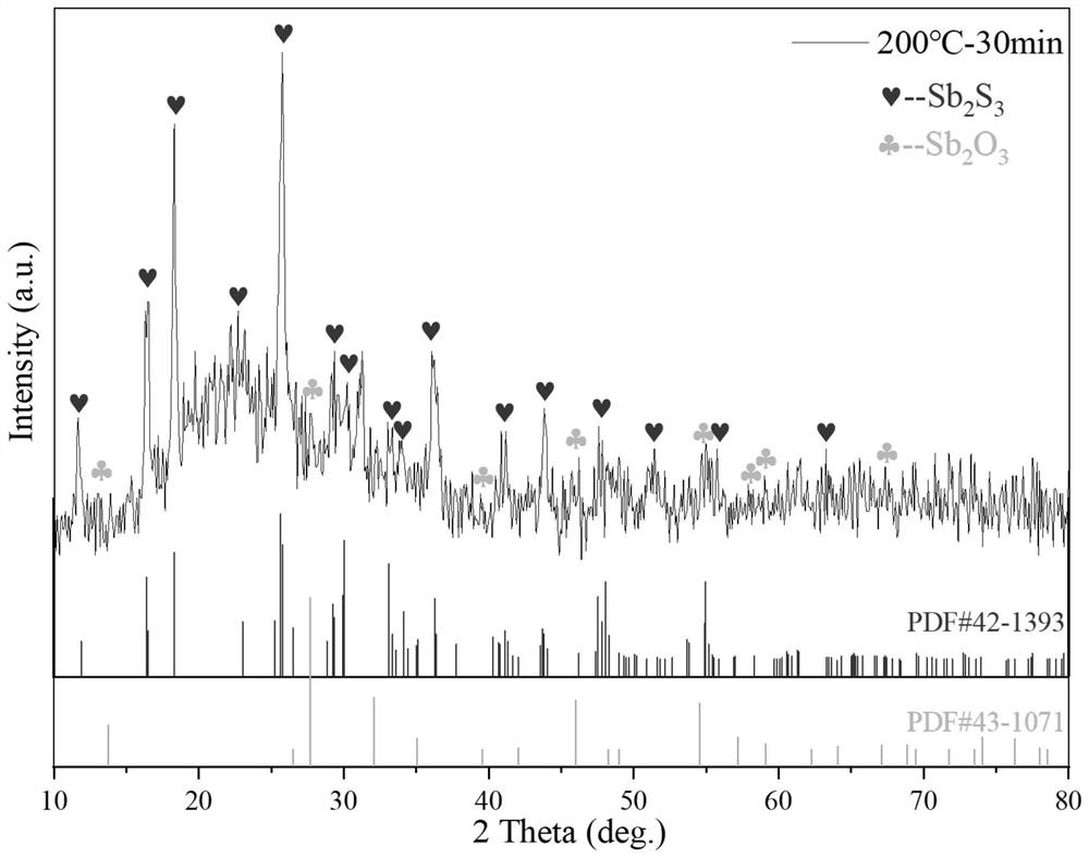
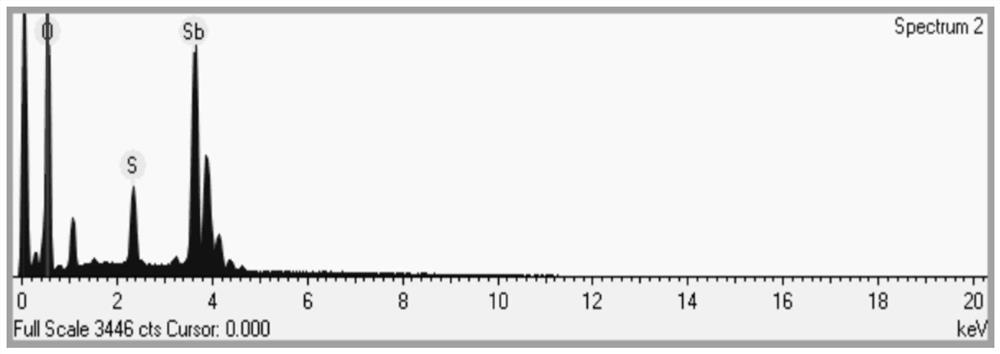
  • Antimony-based photocathode Sb2S3/Sb2O3 heterojunction structure and preparation method thereof
  • Antimony-based photocathode Sb2S3/Sb2O3 heterojunction structure and preparation method thereof
  • Antimony-based photocathode Sb2S3/Sb2O3 heterojunction structure and preparation method thereof

Examples


Embodiment 1

[0031] Embodiment 1: A kind of antimony-based photocathode Sb 2 S 3 / Sb 2 o 3 heterojunction structure, consisting of p-type Sb 2 S 3 Thin film bottom layer, Sb 2 S 3 / Sb 2 o 3 buffer layer and n-type Sb 2 o 3 Composition of the top layer of the film;

[0032] Antimony-based photocathode Sb 2 S 3 / Sb 2 o 3 The preparation method of the heterojunction structure, the preparation of the metal Sb film adopts the vapor phase deposition method, the Sb source is selected from high-purity metal Sb powder, and the substrate is selected from ITO; Sb 2 S 3 The preparation adopts the heating method, and the S source is selected from solid sublimated sulfur; Sb 2 S 3 / Sb 2 o 3 Heterojunction is prepared by heating method; the specific steps are as follows:

[0033] (1) Sputtering Sb on the substrate to obtain Sb film: 5g high-purity metal antimony powder is packed in a crucible, placed in a tube furnace, and the cleaned ITO substrate is placed above the antimony powder ...

Embodiment 2

[0037] Embodiment 2: A kind of antimony-based photocathode Sb 2 S 3 / Sb 2 o 3 heterojunction structure, consisting of p-type Sb 2 S 3 Thin film bottom layer, Sb 2 S 3 / Sb 2 o 3 buffer layer and n-type Sb 2 o 3 Composition of the top layer of the film;

[0038] Antimony-based photocathode Sb 2 S 3 / Sb 2 o 3 The preparation method of the heterojunction structure, the preparation of the metal Sb film adopts the magnetron sputtering method, the Sb source is selected from high-purity metal Sb powder, and the substrate is selected from ITO; Sb 2 S 3 The preparation adopts the PECVD method, and the S source is selected from H 2 S; Sb 2 S 3 / Sb 2 o 3 The heterojunction is prepared by PECVD method; the specific steps are as follows:

[0039] (1) Sputtering Sb on the substrate to obtain Sb thin film: place the high-purity metal antimony target (≥99.99%) on the metal target seat in the magnetron sputtering furnace cavity; after cleaning, the ITO is inverted on the ma...

Embodiment 3

[0043] Embodiment 3: A kind of antimony-based photocathode Sb 2 S 3 / Sb 2 o 3 heterojunction structure, consisting of p-type Sb 2 S 3 Thin film bottom layer, Sb 2 S 3 / Sb 2 o 3 buffer layer and n-type Sb 2 o 3 Composition of the top layer of the film;

[0044] Antimony-based photocathode Sb 2 S 3 / Sb 2 o 3 The preparation method of the heterojunction structure, the preparation of the metal Sb film adopts the vapor phase deposition method, the Sb source is selected from high-purity metal Sb powder, and the substrate is selected from FTO; Sb 2 S 3 The preparation adopts the plasma method, and the S source is selected from solid sublimated sulfur; Sb 2 S 3 / Sb 2 o 3 The heterojunction is prepared by PECVD method; the specific steps are as follows:

[0045] (1) Sputtering Sb on the substrate to obtain Sb film: 5g high-purity metal antimony powder is packed in a crucible, placed in a tube furnace, and the cleaned ITO substrate is placed above the antimony powder...


PUM

PropertyMeasurementUnit
band gapaaaaaaaaaa

Abstract

The invention relates to an antimony-based photocathode Sb2S3 / Sb2O3 heterojunction structure and a preparation method thereof, and belongs to the technical field of photoelectric materials. The antimony-based photocathode Sb2S3 / Sb2O3 heterojunction structure is composed of a p-type Sb2S3 thin film bottom layer, an Sb2S3 / Sb2O3 buffer layer and an n-type Sb2O3 thin film top layer, Sb is sputtered on the substrate to obtain an Sb thin film, the Sb thin film is subjected to a vulcanization reaction to obtain an Sb2S3 thin film, and the Sb2S3 thin film reacts with oxygen to generate an Sb2S3 / Sb2O3 buffer layer and an n-type Sb2O3 conduction band bottom to obtain the Sb2S3 / Sb2O3 heterojunction structure of the antimony-based photocathode. The narrow-band-gap p-type Sb2S3 thin film absorbs light energy, the wide-band-gap Sb2O3 thin film serves as a transmission channel, a catalytic layer and a corrosion-resistant layer of photo-generated electrons, photo-generated carriers are separated by means of the energy range difference between Sb2S3 / Sb2O3 heterojunctions, and the Sb2S3 / Sb2O3 buffer layer improves the charge transmission efficiency and stability and enhances the conductivity of the electrode and the corrosion resistance of the material.

Description

technical field [0001] The invention relates to an antimony-based photocathode Sb 2 S 3 / Sb 2 o 3 The invention relates to a method for preparing a heterojunction structure, which belongs to the technical field of photoelectric materials. Background technique [0002] Antimony sulfide (Sb 2 S 3 ) crystal structure belongs to orthorhombic stibnite structure, which is a kind of green, non-toxic, abundant reserves (Sb crustal abundance is 0.2ppm), and cheap material. Sb 2 S 3 It is a P-type semiconductor with a direct band gap, and its forbidden band width is related to the crystal state of the material. Its band gap is 1.72eV, Ec=0.22V (VS.NHE), Ev=1.94V (VS.NHE). The shortwave absorption coefficient reaches 1.8×10 5 cm -1 . Therefore, only a thickness of about 600nm is needed to fully absorb sunlight on the radiating surface. On the one hand, the amount of materials used is reduced, on the other hand, the migration / diffusion distance of carriers is shortened, and t...

Claims


Application Information

Patent Timeline
Patent Type & Authority Applications(China)
IPC IPC(8): H01L31/0336H01L31/0352H01L31/036H01L31/0392H01L31/18
CPCH01L31/0336H01L31/036H01L31/0392H01L31/035272H01L31/18Y02P70/50
Inventor 杨佳张君杨海艳王薇侯堪文黄滔张雅婷徐宝强李绍元杨斌马文会熊恒刘大春李一夫田阳蒋文龙戴永年
Owner KUNMING UNIV OF SCI & TECH
Learn More