Multi-epitaxy super junction power MOSFET structure and use method

A power and epitaxy technology, used in electrical components, fire rescue, electrical solid devices, etc., can solve the problems of easy bending of electrode columns, unsealed shells, easy to loosen and fall off, etc., to improve breakdown voltage and performance, and strengthen connection strength. , Improve the effect of interface characteristics

Pending Publication Date: 2021-11-23
厦门芯一代集成电路有限公司
View PDF1 Cites 2 Cited by
  • Summary
  • Abstract
  • Description
  • Claims
  • Application Information

AI Technical Summary

Problems solved by technology

[0008] The purpose of the present invention is to solve the shortcomings existing in the prior art, such as: characteristics, breakdown voltage performance cannot be improved as a whole, heat dissipation is blocked or poor, the shell is not sealed and the electrode column is easy to bend, and it is easy to loosen and fall off after being connected to the circuit , and proposed a multi-epitaxial super-junction power MOSFET structure and its application method

Method used


Image

  • Multi-epitaxy super junction power MOSFET structure and use method
  • Multi-epitaxy super junction power MOSFET structure and use method
  • Multi-epitaxy super junction power MOSFET structure and use method

Examples


Embodiment Construction

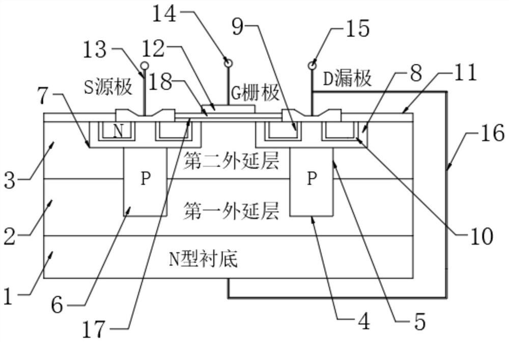
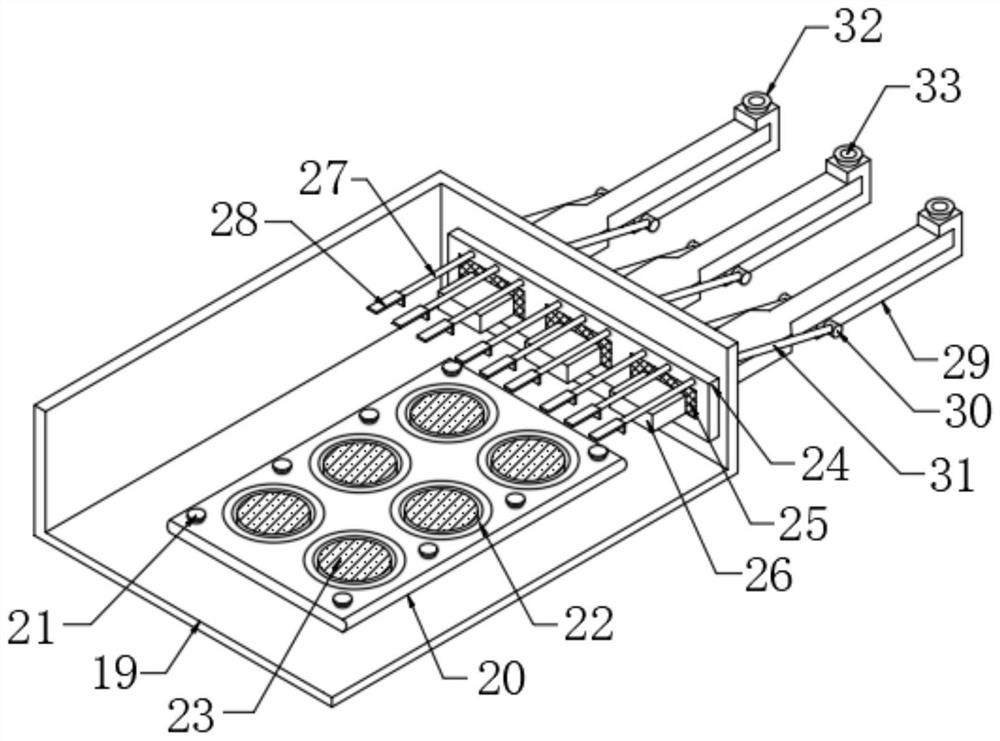
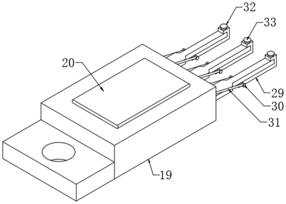
[0033] The following will clearly and completely describe the technical solutions in the embodiments of the present invention with reference to the accompanying drawings in the embodiments of the present invention. Obviously, the described embodiments are only some, not all, embodiments of the present invention. Based on the embodiments of the present invention, all other embodiments obtained by persons of ordinary skill in the art without creative efforts fall within the protection scope of the present invention.

[0034] In describing the present invention, it should be understood that the terms "upper", "lower", "front", "rear", "left", "right", "top", "bottom", "inner", " The orientation or positional relationship indicated by "outside", etc. is based on the orientation or positional relationship shown in the drawings, and is only for the convenience of describing the present invention and simplifying the description, rather than indicating or implying that the referred dev...


PUM


Abstract

The invention discloses a multi-epitaxy super junction power MOSFET structure and a use method, and relates to the technical field of semiconductor field effect transistors. The multi-epitaxy super junction power MOSFET structure comprises an N-type substrate and a shell, the substrate is arranged in the shell, and the top end of the N-type substrate is fixedly connected with a first epitaxial layer; the top end of the first epitaxial layer is fixedly connected with a second epitaxial layer, two grooves are formed in the top end of the first epitaxial layer, and two through grooves are formed in the middle of the second epitaxial layer. According to the present invention, the N-type substrate is arranged, the first epitaxial layer is formed on the surface of the N-type substrate by means of an epitaxial process, the top end of the first epitaxial layer is etched to form the two grooves, a gate oxide layer is formed in the middle of the surface of the second epitaxial layer, and a polycrystalline silicon grid electrode is formed on the surface of the gate oxide layer, so that the design of double-layer epitaxy or even multi-layer epitaxy can be realized, the breakdown voltage and performance of an MOSFET can be greatly improved, the ideal resistivity matching exists between two layers or multiple layers, and the interface characteristics of the multiple stacked epitaxial layers can be improved.

Description

technical field [0001] The invention relates to the technical field of semiconductor field effect transistors, in particular to a multiple epitaxial super junction power MOSFET structure and a use method. Background technique [0002] Metal-Oxide Semiconductor Field-Effect Transistor, referred to as Metal-Oxide-Semiconductor Field-Effect Transistor (MOSFET), is a field-effect transistor that can be widely used in analog circuits and digital circuits. Looking at the naming of MOSFETs from a different perspective, it will actually give people the wrong impression. Because the first letter M representing "metal" in MOSFET does not exist in most of the current similar components. The gate electrode of the early MOSFET uses metal as its material, but with the advancement of semiconductor technology, the gate electrode of the MOSFET uses polysilicon instead of metal. In the processor, the polysilicon gate is no longer the mainstream technology. Starting from Intel's P1266 proces...

Claims


Application Information

Patent Timeline
IPC IPC(8): H01L23/16H01L23/24H01L23/367H01L23/373H01L29/06H01L29/423H01L23/00H01L29/78H01L21/336H01L21/28A62C3/16
CPCH01L29/78H01L29/66477H01L29/0684H01L29/0615H01L29/0634H01L29/401H01L29/42356H01L23/562H01L23/3672H01L23/373H01L23/367H01L23/16H01L23/24A62C3/16
Inventor 陈利陈彬
Owner 厦门芯一代集成电路有限公司
Why Eureka
Try Eureka