SOI LDMOS device capable of improving self-heating effect

A self-heating effect and device technology, applied in semiconductor devices, electrical components, circuits, etc., can solve the problems of hindering heat release, total dose effect, etc., to reduce the amount of collection, improve the overall performance, and ensure the performance of anti-single particle burnout Effect

Pending Publication Date: 2021-12-10
江苏芯唐微电子有限公司
View PDF0 Cites 0 Cited by
  • Summary
  • Abstract
  • Description
  • Claims
  • Application Information

AI Technical Summary

Problems solved by technology

However, since the thermal conductivity of the buried oxide layer is much lower than that of the silicon substrate, for example, the thermal conductivity of silicon dioxide is 1.4W/m.K, while that of silicon is 140W/m.K, so the buried oxide layer

Method used


Image

  • SOI LDMOS device capable of improving self-heating effect
  • SOI LDMOS device capable of improving self-heating effect
  • SOI LDMOS device capable of improving self-heating effect

Examples


Embodiment Construction

[0016] The specific embodiments of the present invention will be further described below in conjunction with the accompanying drawings.

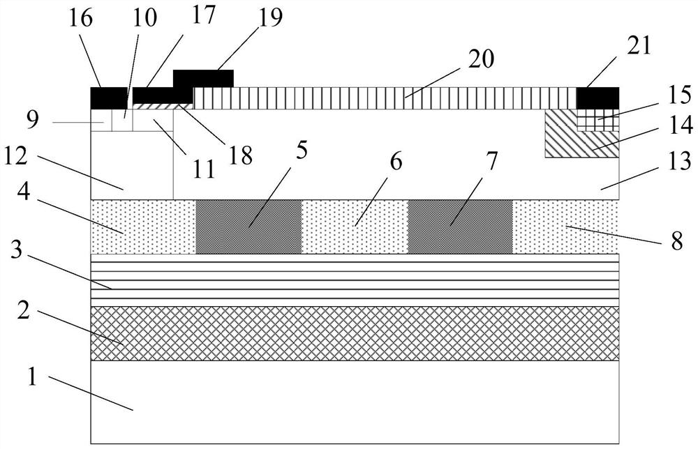
[0017] This application discloses a SOI LDMOS device that improves the self-heating effect, please refer to figure 1 , the SOI LDMOS device includes a substrate silicon layer 1, a P-type heavily doped silicon layer 2, an N-type lightly doped semiconductor layer 3 and an active region structure, and the P-type heavily doped silicon layer 2 is stacked on the substrate silicon layer 1, the N-type lightly doped semiconductor layer 3 is stacked on the P-type heavily doped silicon layer 2, and the active region structure is set on the N-type lightly doped semiconductor layer 3, and the N-type lightly doped semiconductor layer 3 adopts a wide Made of forbidden material. Wherein, the heavy doping and light doping of the P-type heavily doped silicon layer 2 and the N-type lightly doped semiconductor layer 3 are relative, and there is no specific dop...


PUM


Abstract

The invention discloses an SOI LDMOS device for improving a self-heating effect, which relates to the field of SOI devices, and adopts a P-type heavily doped silicon layer and an N-type lightly doped semiconductor layer which are stacked to replace a conventional buried oxide layer, so that the dielectric isolation effect of the buried oxide layer can also be realized; and the thermal conductivity of the silicon layer and the semiconductor layer is much higher than that of the conventional buried oxide layer, so that the self-heating effect can be improved on the basis that the SOI LDMOS device has the advantages of high speed and low power consumption.

Description

technical field [0001] The invention relates to the field of SOI devices, in particular to an SOI LDMOS device with improved self-heating effect. Background technique [0002] Compared with traditional bulk silicon devices, SOI LDMOS (Silicon-on-Insulator Laterally Double-Diffused MOSFET) devices introduce a thick buried oxide layer between the active region and the substrate to achieve dielectric isolation, making SOI LDMOS The device has the advantages of fast speed and low power consumption, and is widely used in various electronic power systems. However, since the thermal conductivity of the buried oxide layer is much lower than that of the silicon substrate, for example, the thermal conductivity of silicon dioxide is 1.4W / m.K, while that of silicon is 140W / m.K, so the buried oxide layer is equivalent to a heat sink. The barrier layer hinders the release of heat from the active region to the substrate, which will also cause serious total dose effects and self-heating ef...

Claims


Application Information

Patent Timeline
IPC IPC(8): H01L29/78H01L29/10
CPCH01L29/7824H01L29/1079
Inventor 杨洋
Owner 江苏芯唐微电子有限公司
Why Eureka
Try Eureka