Composite substrate based on aluminum nitride ceramic material and preparation method and application of composite substrate
A technology of aluminum nitride ceramics and composite substrates, applied in semiconductor/solid-state device manufacturing, electrical components, electrical solid-state devices, etc., can solve problems such as GaN or AlN single crystal substrates, and achieve thermal conductivity advantages Obvious, improved thermal conductivity, and reduced dislocation density
- Summary
- Abstract
- Description
- Claims
- Application Information
AI Technical Summary
Problems solved by technology
Method used
Image

Examples
Embodiment 1
[0063] This embodiment is used to illustrate the composite substrate of the present invention and its preparation method.
[0064] (1) Select a high-quality AlN ceramic substrate with a thickness of 500 microns (Zhongchuang Yanyuan Semiconductor Technology Co., Ltd., 180W / mk aluminum nitride ceramic substrate), and use the CMP polishing method to polish the surface of the AlN ceramic substrate. Obvious steps, surface roughness within 25nm;
[0065] (2) Using PECVD technology to grow SiO on the polished surface of the above ceramic substrate 2 thin film, SiO 2 The film thickness is 2.0 microns;
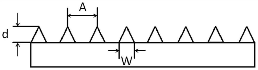
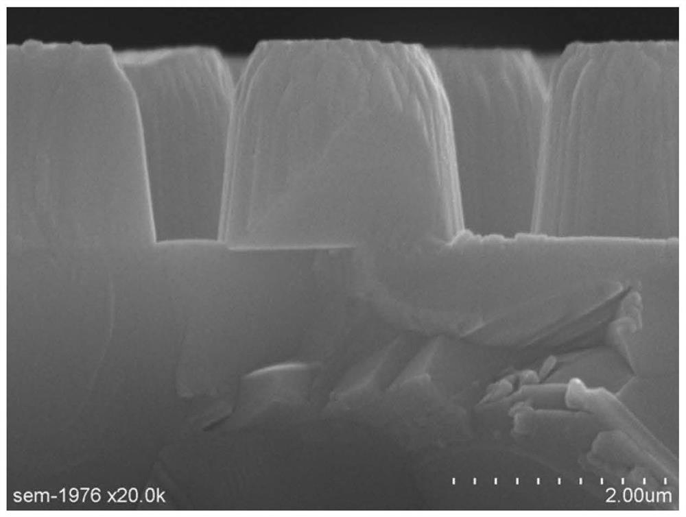
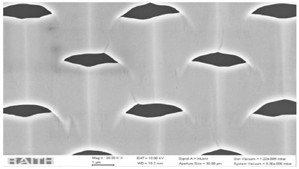
[0066] (3) Use a glue spreader to coat the above SiO 2 The surface is coated with a photoresist with a thickness of 1.2 microns, and the photoresist is imprinted into a periodic cylinder with a bottom diameter of 2 μm, a height of about 2.4 μm, and a period of 3 μm by using nano-imprint technology; using ICP etching technology to etch The AlN ceramic substrate after imprinting, the S...
Embodiment 2
[0073] This embodiment is used to illustrate the composite substrate of the present invention and its preparation method.
[0074] (1) Select a high-quality AlN ceramic substrate with a thickness of 500 microns (Zhongchuang Yanyuan Semiconductor Technology Co., Ltd. 180W / mk aluminum nitride ceramic substrate), and use CMP polishing to polish the surface of the AlN ceramic substrate. The microscope shows that the surface is not obvious Steps, surface roughness within 5nm;
[0075] (2) Using PECVD technology to grow SiO on the polished surface of the above ceramic substrate 2 thin film, SiO 2 The film thickness is 1.5 microns;
[0076] (3) Use a glue spreader to coat the above SiO 2 The surface is coated with a photoresist with a thickness of 1.2 microns, and the photoresist is imprinted into a periodic cylinder with a bottom diameter of 2 μm, a height of about 2.4 μm, and a period of 3 μm by using nano-imprint technology; using ICP etching technology to etch The AlN ceramic...
Embodiment 3
[0085] This embodiment is used to illustrate the composite substrate of the present invention and its preparation method.
[0086] (1) Select a high-quality AlN ceramic substrate with a thickness of 200 microns (Nippon Maruwa Co., Ltd. 180W / mk aluminum nitride ceramic substrate), and use CMP polishing to polish the surface of the AlN ceramic substrate. The microscope shows that there are no obvious steps on the surface and the surface is rough. The degree is within 0.01nm;
[0087] (2) Using PECVD technology to grow SiO on the polished surface of the above ceramic substrate 2 thin film, SiO 2 The film thickness is 1.5 microns;
[0088] (3) Use a glue spreader to coat the above SiO 2 The surface is coated with a photoresist with a thickness of 1.2 microns, and the photoresist is imprinted into a periodic cylinder with a bottom diameter of 2 μm, a height of about 2.4 μm, and a period of 3 μm by using nano-imprint technology; using ICP etching technology to etch The AlN ceram...
PUM
| Property | Measurement | Unit |
|---|---|---|
| thickness | aaaaa | aaaaa |
| surface roughness | aaaaa | aaaaa |
| thickness | aaaaa | aaaaa |
Abstract
Description
Claims
Application Information
 - R&D
- Intellectual Property
- Life Sciences
- Materials
- Tech Scout
- Unparalleled Data Quality
- Higher Quality Content
- 60% Fewer Hallucinations
Browse by: Latest US Patents, China's latest patents, Technical Efficacy Thesaurus, Application Domain, Technology Topic, Popular Technical Reports.
© 2025 PatSnap. All rights reserved.Legal|Privacy policy|Modern Slavery Act Transparency Statement|Sitemap|About US| Contact US: help@patsnap.com