Preparation method of perovskite material layer and battery device
A perovskite material and perovskite technology, applied in the direction of electrical solid devices, electrical components, semiconductor devices, etc., can solve the problems of poor transmission, strong electron recombination at grain boundaries, and affecting the performance of battery devices, so as to prevent charge recombination, Improvement of extraction and transfer, the effect of increasing the efficiency of battery devices
- Summary
- Abstract
- Description
- Claims
- Application Information
AI Technical Summary
Problems solved by technology
Method used
Image

Examples
preparation example Construction
[0020] The application provides a method for preparing a perovskite material layer, comprising the following steps:
[0021] S1. A perovskite solution is obtained from a solute and a solvent configuration, the solute includes a precursor material or perovskite single crystal, N-type or P-type nano-conductive particles prepared by it; the precursor material includes PbI 2 , PbBr 2 , CsI or CsBr; the N-type nano conductive particles are fullerene, SnO 2 、TiO 2 or ZnO nanoparticles; the P-type nano-conductive particles are NiO x 、Cu 2 Nanoparticles of O, CuI or CuSCN;
[0022] S2, wet-forming the perovskite solution obtained in step S1, and then performing annealing treatment at an annealing temperature of 100-150° C. for 10-30 minutes to form a perovskite crystal layer with a thickness of 100-300 nm, and There are channels at the grain boundaries;
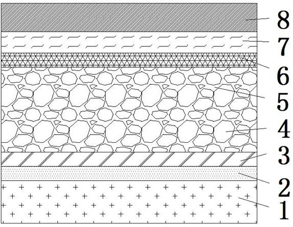
[0023] S3, forming a barrier layer for preventing charge recombination on the surface of the perovskite crystal layer obtaine...
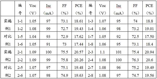
Embodiment 1
[0042] A method for preparing a perovskite material layer and a battery device, specifically as follows:
[0043] (1) Configure the perovskite precursor solution according to MAPbI 3 Stoichiometric ratio, MAI:PbI 2 =1:1 (molar ratio), perovskite concentration 1mol / L, solvent DMF; add N-type nano conductive particles: SnO 2 Nanoparticles, 0.1% by mole ratio of perovskite.
[0044] (2) Preparation of SnO by spin-coating method on FTO conductive substrate 2 Electron transport layer, thickness 40nm, SnO 2 The precursor solution is commercially available SnO 2 Colloidal dispersion, its ratio is dispersion: ultrapure water = 1:3 (volume ratio).
[0045] (3) SnO prepared in step (2) 2 On the electron transport layer, the perovskite solution obtained in step (1) was prepared into a film by scraping coating method, and then annealed. 2 Nanoparticles are enriched at the grain boundary to form N-type channels;
[0046] (4) On the perovskite crystalline layer prepared in step (3),...
Embodiment 2
[0052] A method for preparing a perovskite material layer and a battery device, specifically as follows:
[0053] (1) Configure the perovskite precursor solution, using perovskite Cs 0.05 FA 0.70 MA 0.25 PB 3 , concentration 1.2mol / L, solvent DMF:DMSO=9:1 (volume ratio); add P-type nano conductive particles: NiO x Nanoparticles, 0.15% by mole ratio of perovskite.
[0054] (2) Use NiO on the FTO conductive substrate x A pure aqueous solution of nanoparticles was used to prepare a hole transport layer with a thickness of 50 nm by spin coating, and annealed at 120° C. for 10 min.
[0055] (3) On the hole transport layer prepared in step (2), the perovskite solution obtained in step (1) was prepared into a film by scraping coating method, and then annealed. The annealing temperature was 150°C and the time was 20 minutes. Thickness 250nm, while NiO x Nanoparticles are enriched at the grain boundary to form P-type channels;
[0056] (4) On the perovskite crystal layer prepar...
PUM
| Property | Measurement | Unit |
|---|---|---|
| thickness | aaaaa | aaaaa |
| thickness | aaaaa | aaaaa |
| thickness | aaaaa | aaaaa |
Abstract
Description
Claims
Application Information
 - Generate Ideas
- Intellectual Property
- Life Sciences
- Materials
- Tech Scout
- Unparalleled Data Quality
- Higher Quality Content
- 60% Fewer Hallucinations
Browse by: Latest US Patents, China's latest patents, Technical Efficacy Thesaurus, Application Domain, Technology Topic, Popular Technical Reports.
© 2025 PatSnap. All rights reserved.Legal|Privacy policy|Modern Slavery Act Transparency Statement|Sitemap|About US| Contact US: help@patsnap.com