
TSV-combined electroplating pretreatment process method

A technology of electroplating pretreatment and process method, which is applied in the direction of circuits, electrical components, semiconductor devices, etc., can solve problems such as copper seed layer electroplating defects, and achieve the effects of easy control, large process window, and reduced scrap

Pending Publication Date: 2022-01-07
新阳硅密(上海)半导体技术有限公司
View PDF4 Cites 0 Cited by
  • Summary
  • Abstract
  • Description
  • Claims
  • Application Information

AI Technical Summary

Problems solved by technology

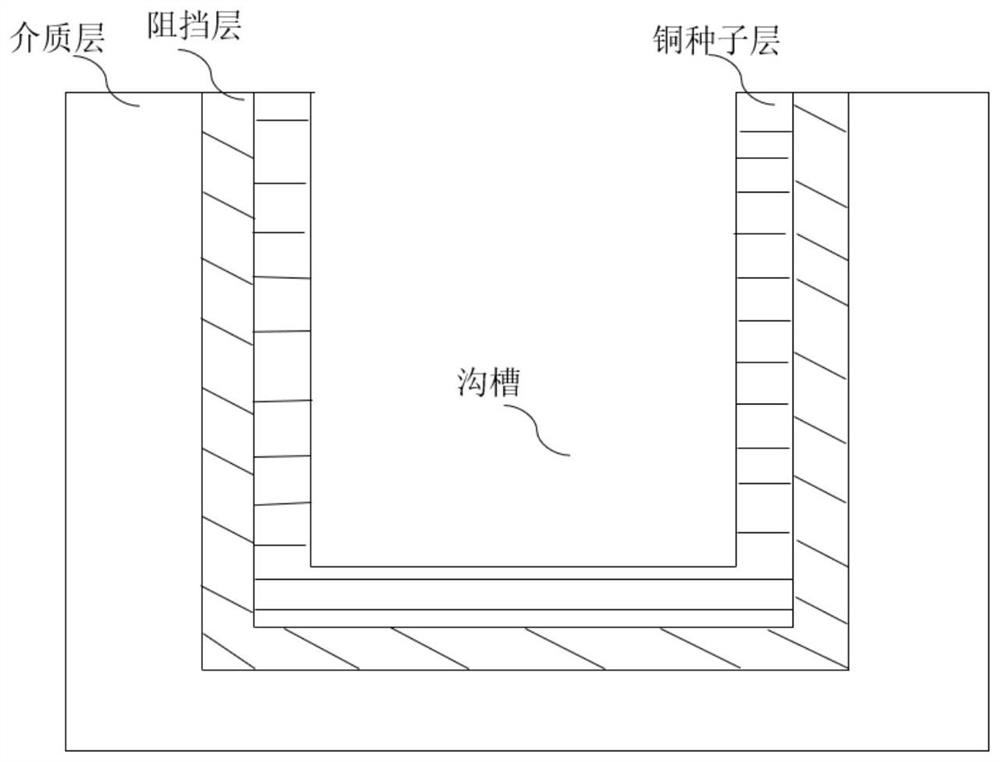
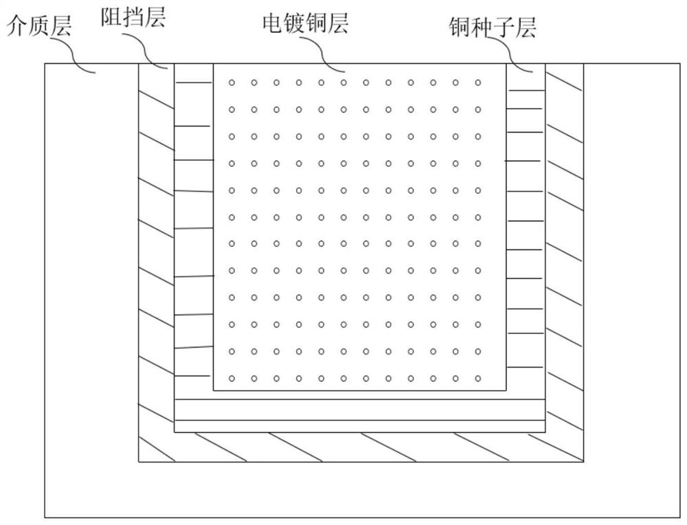
[0008] For the defects in the prior art, the purpose of the present invention is to provide a kind of combined TSV electroplating pretreatment process method, to solve the electroplating defect problem caused by copper seed layer surface defects (such as oil stains, oxidation, etc.) existing in the prior art

Method used


Image

  • TSV-combined electroplating pretreatment process method
  • TSV-combined electroplating pretreatment process method
  • TSV-combined electroplating pretreatment process method

Examples


no. 1 example

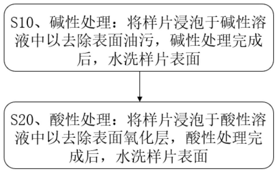
[0049] like image 3 As shown, this embodiment provides a method for combining TSV electroplating pretreatment process, including the following steps:

[0050] S10. Alkaline treatment: soak the sample in alkaline solution to remove surface oil, after the alkaline treatment is completed, wash the surface of the sample;

[0051] S20. Acid treatment: soak the sample in an acidic solution to remove the surface oxide layer, and wash the surface of the sample with water after the acid treatment is completed.

[0052] In the above steps, step S10, that is, the alkaline treatment step, can effectively remove the oil stain on the surface of the sample, and make the surface of the sample and the acidic electroplating solution more bonded; step S20, that is, the acidic treatment step, can effectively remove the oxide layer on the surface of the sample, thereby Avoid the electroplating defect problem caused by the oxidation problem in the wafer electroplating, and reduce the scrapping of...

no. 2 example

[0055] like Figure 4 As shown, this embodiment provides a method for combining TSV electroplating pretreatment process, including the following steps:

[0056] S10. Alkaline treatment: Soak the sample in an alkaline solution to remove surface oil. The alkaline solution is KOH solution or NaOH solution. The pH value of the alkaline solution is between 7 and 13. After the alkaline treatment is completed, wash with water sample surface;

[0057] S20. Acid treatment: soak the sample in an acid solution to remove the surface oxide layer. The acid solution is a mixture of 0.3% to 5% sulfuric acid and hydrogen peroxide. After the acid treatment, the surface of the sample is washed with water.

[0058] The important difference between this embodiment and the first embodiment is that this embodiment specifically defines that the alkaline solution used is KOH solution or NaOH solution, and the acidic solution is a mixture of sulfuric acid and hydrogen peroxide, wherein KOH solution or...

no. 3 example

[0060] like Figure 5 As shown, this embodiment provides a method for combining TSV electroplating pretreatment process, including the following steps:

[0061] S10. Alkaline treatment: soak the sample in an alkaline solution under vacuum conditions to remove surface oil, and wash the surface of the sample with water after the alkaline treatment is completed;

[0062] S20. Acid treatment: soak the sample in an acidic solution under vacuum conditions to remove the surface oxide layer, and wash the surface of the sample with water after the acid treatment is completed.

[0063] The difference between this embodiment and the first embodiment is that this embodiment limits the alkali treatment and acid treatment steps under vacuum conditions, thus having the beneficial effect that the vacuum conditions can extract the air in the sample groove, Therefore, it is beneficial for the alkaline solution and the acidic solution to enter into it, thereby achieving the purpose that the alk...


PUM


Abstract

The invention provides a TSV-combined electroplating pretreatment process method. The TSV-combined electroplating pretreatment process method comprises the following steps of S10, alkaline treatment, wherein a sample wafer is soaked in an alkaline solution to remove surface oil stains, and after alkaline treatment is completed, the surface of the sample wafer is washed with water; and S20, acidic treatment, wherein the sample wafer is soaked in an acidic solution to remove a surface oxide layer, and after acidic treatment is completed, the surface of the sample wafer is washed with water. According to the TSV-combined electroplating pretreatment process method, the alkaline treatment step can effectively remove the oil stains on the surface of the sample wafer, and the surface of the sample wafer is more attached to the acidic electroplating solution; the acidic treatment step can effectively remove the surface oxide layer of the sample wafer, so that the problem of electroplating defects caused by oxidation in wafer electroplating is avoided, and the scrap of wafers is reduced; and the alkaline treatment step and the acidic treatment step are combined, so that the conductivity of a seed layer of the sample wafer is guaranteed, the smooth operation of a subsequent electroplating process is facilitated, and particularly for some sample wafers which cannot be subjected to the electroplating process in time or are stored for a long time, the yield of electroplating products is greatly improved.

Description

technical field [0001] The invention relates to the technical field of microelectronic packaging, in particular to a pretreatment process combined with TSV electroplating. Background technique [0002] Through Silicon Via (TSV for short) is a high-density packaging technology that is gradually replacing the current more mature wire bonding technology and is considered to be the fourth-generation packaging technology. TSV technology realizes the vertical electrical interconnection of through-silicon holes by filling conductive substances such as copper, tungsten, and polysilicon. The TSV development process includes making vertical via holes on the wafer by etching, laser drilling, etc., and then making insulating layers, barrier layer and seed layer deposition, filling metal, chemical mechanical polishing, thinning and Subsequent wafer bonding steps. [0003] In the integrated circuit industry, the traditional circuit material is generally aluminum, but with the reduction ...

Claims


Application Information

Patent Timeline
IPC IPC(8): C25D7/12C23G1/10C23G1/20C25D5/02C25D5/34H01L21/768
CPCC25D7/123C25D5/34C25D5/02C23G1/20C23G1/103H01L21/76898H01L21/76879
Inventor 史蒂文·贺·汪刘立安
Owner 新阳硅密(上海)半导体技术有限公司
Learn More