

Top gate structure all-solid-state memory transistor multivariable mask plate based on overlay technology
A mask and sub-mask technology, which is applied in the field of multi-variable masks of top-gate structure all-solid-state memory transistors, can solve the problems of unfavorable experimental data, difficult degradation, and high cost, and achieves simple equipment, easy control, and film formation. good effect
- Summary
- Abstract
- Description
- Claims
- Application Information
AI Technical Summary
Problems solved by technology
Method used
Image

Examples
Embodiment 1
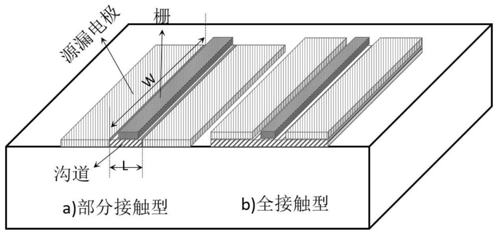
[0051] Table 1 shows the two contact types of this embodiment and the eight different device sizes they contain: pure numbers indicate full contact devices, and numbers marked with "'" indicate partial contact devices.
[0052] Table 1
[0053]
[0054] figure 1 It is a diagram of the contact mode between the source and drain electrodes and the channel according to the device of this embodiment. Divided into full contact type and partial contact type, the purpose is to compare the influence of parasitic parameters between source-drain electrodes and channels on device performance.
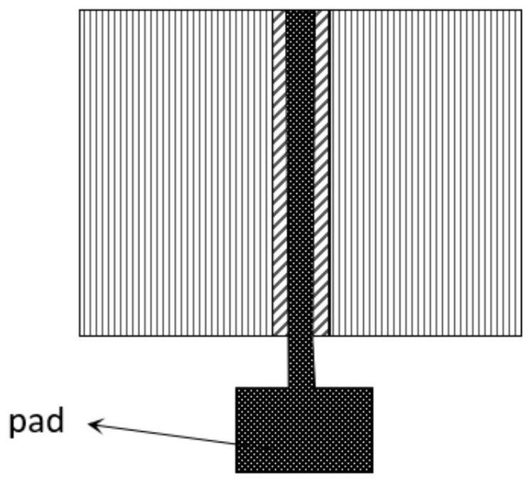
[0055] figure 2 For some devices with a small gate size in this embodiment, it is necessary to draw an illustration of the Pad area for needle sticking. Because the diameter of the probe of the Keithley semiconductor tester is 10 μm, for the convenience of testing.
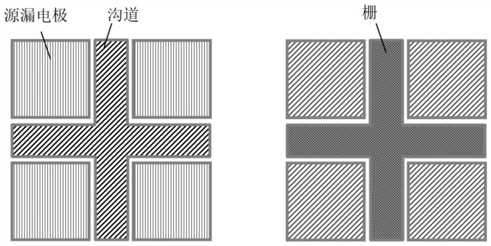
[0056] image 3 It is a diagram of the position of the registration mark in the mask plate (channel mask plate, source-drain...
Embodiment 2
[0140] With embodiment 1, difference is, the Li of grid electrolyte in the step (11) 3 PO 4 Change target sputtering atmosphere to N 2 , the power was changed to 38W, the time was 5400s, and 100nm thick LiPON was plated.
[0141] It has been verified by experiments that LiPON is more 3 PO 4 There is a more obvious advantage that the ionic conductivity of LiPON is higher than that of Li 3 PO 4 much higher.
[0142] In order to avoid the problem of process accuracy, in the preparation process of the above embodiments, each contact surface is overlapped by 3 μm to prevent gaps.
[0143] Effect verification:
[0144] (1) In Example 1, the channel material WO was prepared sequentially through photolithography-coating-exposure-development-sputtering-stripping 3 (blue) and source-drain electrode material Au (golden yellow), observe the micrograph ( Image 6 with Figure 7 ),in Image 6 It is a photomicrograph figure of the step (1) device in the effect verification of the ...
PUM
| Property | Measurement | Unit |
|---|---|---|
| thickness | aaaaa | aaaaa |
| thickness | aaaaa | aaaaa |
Abstract
Description
Claims
Application Information