Solar cell and preparation method thereof

A solar cell and electrode technology, applied in the field of solar cells, can solve the problems of increasing parasitic light absorption, reducing light utilization efficiency, and low content, and achieve the effects of improving light utilization efficiency, reducing parasitic light absorption, and reducing manufacturing costs

Pending Publication Date: 2022-02-01
JA SOLAR TECH YANGZHOU
View PDF0 Cites 1 Cited by
  • Summary
  • Abstract
  • Description
  • Claims
  • Application Information

AI Technical Summary

Problems solved by technology

However, due to the low content of silver in the earth's crust and the relatively high price, the production cost of solar cells is relatively high; at the same time, since it is often necessary to corrode part of the silicon through the glass frit in the silver paste to form an ohmic contact, the junction depth requirements for diffusion Deeper, if used to passivate contact cells, a thicker polysilicon layer is required
If aluminum paste is used instead of silver paste to reduce costs, it is difficult to ensure that the thin polysilicon layer will not be damaged when the glass frit in aluminum paste reacts with silicon under high temperature conditions
The thicker polysilicon layer not only increases the manufacturing cost of solar cells, but also increases the parasitic light absorption, reduces the light utilization efficiency, and limits the efficiency of solar cells.

Method used


Image

  • Solar cell and preparation method thereof
  • Solar cell and preparation method thereof
  • Solar cell and preparation method thereof

Examples


preparation example Construction

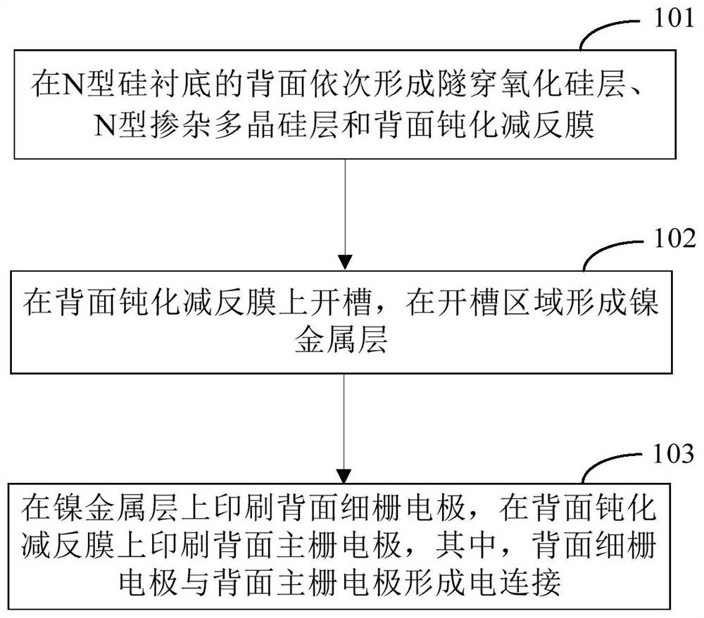
[0045] In order to solve the above problems, an embodiment of the present invention provides a method for manufacturing a solar cell. in, figure 1 A schematic diagram of the main flow of the solar cell fabrication method. Such as figure 1 As shown, the preparation method of the solar cell may include the following steps:

[0046] Step 101, sequentially forming a tunneling silicon oxide layer 2, an N-type doped polysilicon layer 4 and a rear passivation anti-reflection film 5 on the back of the N-type silicon substrate 1;

[0047] Step 102, groove the passivation anti-reflection film 5 on the back surface, and form a nickel metal layer 6 in the grooved area;

[0048] Step 103 , printing the back fine grid electrode 7 a on the nickel metal layer 6 , and printing the rear main grid electrode 7 b on the rear passivation antireflection film 5 , wherein the rear fine grid electrode 7 a is electrically connected to the rear main gate electrode 7 b.

[0049] Wherein, the front sid...

Embodiment 1

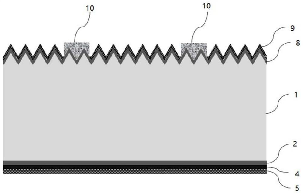
[0093] Step A1: providing an N-type silicon substrate 1 , performing texturing treatment on the front and back sides of the N-type silicon substrate 1 , and performing polishing treatment on the back side of the N-type silicon substrate 1 .

[0094] Step B1: performing boron diffusion treatment on the front side of the N-type silicon substrate 1 to form a P+ emitter 8 .

[0095] Step C1: removing the p-n junction and borosilicate glass on the back of the N-type silicon substrate 1 by using HF acid solution.

[0096] Step D1: Form a tunneling silicon oxide layer 2 with a thickness of 1-2 nm on the back surface of the N-type silicon substrate 1 by high temperature thermal oxidation.

[0097] Step E1: forming an intrinsic polysilicon layer 3 on the tunneling silicon oxide layer 2 on the back side of the N-type silicon substrate 1 by LPCVD / PVD.

[0098] Step F1: doping the intrinsic polysilicon layer 3 on the back side with phosphorus by ion implantation, and performing annealing...

Embodiment 2

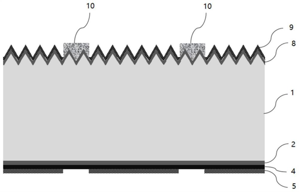
[0107] Step A2-C2: consistent with step A1-C1 provided in Example 1.

[0108] Step D2: Form a tunneling silicon oxide layer 2 with a thickness of 1-2 nm on the back and front of the N-type silicon substrate 1 by high temperature thermal oxidation method.

[0109] Step E2: forming an intrinsic polysilicon layer 3 on the back and front tunnel silicon oxide layers 2 of the N-type silicon substrate 1 by LPCVD / PVD.

[0110] Step F2: doping the intrinsic polysilicon layer 3 on the back side with phosphorus by ion implantation, and performing annealing to form an N-type doped polysilicon layer 4, wherein the N-type doped polysilicon layer has a thickness of 80- Between 200nm.

[0111] Step G2: removing the intrinsic polysilicon layer 3 on the front side of the N-type silicon substrate 1 with potassium hydroxide solution or sodium hydroxide solution, and then removing the tunneling silicon oxide layer 2 and borosilicate glass on the front side with HF acid solution.

[0112] Step H2...


PUM

PropertyMeasurementUnit
thicknessaaaaaaaaaa
thicknessaaaaaaaaaa

Abstract

The invention discloses a solar cell and a preparation method of the solar cell. The preparation method of the solar cell comprises the following steps: sequentially forming a tunneling silicon oxide layer, an N-type doped polycrystalline silicon layer and a back passivation anti-reflection film on the back surface of an N-type silicon substrate; grooving the back passivation anti-reflection film, and forming a nickel metal layer in a grooving area; printing a back fine gate electrode on the nickel metal layer, printing a back main gate electrode on the back passivation anti-reflection film, and electrically connecting the back fine gate electrode with the back main gate electrode. According to the preparation method, the binding force between the metal gate line and silicon can be ensured, meanwhile, the damage of the slurry to the thin polycrystalline silicon layer in the using process is avoided, the passivation effect of the passivation contact structure is ensured, the manufacturing cost of the solar cell is reduced, parasitic light absorption is reduced, and the light utilization efficiency is improved. And the efficiency of the solar cell is improved.

Description

technical field [0001] The invention relates to a solar cell and a preparation method of the solar cell. Background technique [0002] PERC (Passivated Emitter and Rear Cell, Passivated Emitter and Rear Cell) solar cells use a silicon oxide layer passivation on the back surface of the silicon substrate, and local openings to achieve point contact to reduce the area of ​​​​the non-passivation area, through local metal contact , greatly reducing the recombination speed of the back surface, while improving the light reflection of the back surface and improving the conversion efficiency of the solar cell. Passivated contact solar cells (such as TOPCon (Tunnel Oxide Passivated Contact, tunneling oxidation passivated contact) solar cells) adopt a passivated contact structure composed of a tunneling silicon oxide layer and a doped polysilicon layer, which can effectively reduce surface recombination and Metal contact compounding improves the conversion efficiency of the battery. ...

Claims


Application Information

Patent Timeline
Patent Type & Authority Applications(China)
IPC IPC(8): H01L31/18H01L31/0224H01L31/068H01L31/0216
CPCH01L31/1804H01L31/1868H01L31/022441H01L31/022433H01L31/068H01L31/02167H01L31/02168Y02E10/546Y02E10/547Y02P70/50
Inventor 蒋秀林陈斌段光亮
Owner JA SOLAR TECH YANGZHOU
Why Eureka
Try Eureka