Silicon carbide diode and preparation method thereof
A silicon carbide diode, silicon carbide technology, used in semiconductor/solid-state device manufacturing, electrical components, circuits, etc., can solve problems such as instability, and achieve the effects of improving uniformity, improving device performance, and high flat top uniformity.
- Summary
- Abstract
- Description
- Claims
- Application Information
AI Technical Summary
Problems solved by technology
Method used
Image
Examples
Embodiment 1
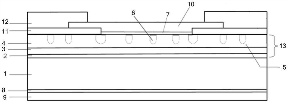
[0057] Such as figure 1 As shown, this embodiment provides a silicon carbide diode, including a silicon carbide substrate 1, a multi-layer epitaxial layer, a plurality of P-type voltage divider rings 5, a plurality of P-type diffusion regions 6, a Schottky barrier layer 7, Ohmic contact layer 8 , back metal electrode 9 , front metal electrode 10 , silicon dioxide film 11 and polyimide layer 12 . Both the back metal electrode 9 and the silicon carbide substrate 1 are arranged on the ohmic contact layer 8, the ohmic contact layer 8 is located between the back metal electrode 9 and the silicon carbide substrate 1, and the multilayer epitaxial layer 13 is arranged on the silicon carbide substrate 1 , the silicon carbide substrate 1 is located between the multilayer epitaxial layer 13 and the ohmic contact layer 8, and both ends of the multilayer epitaxial layer 13 are provided with a silicon dioxide film 11, and the multilayer epitaxial layer 13 is located between the silicon diox...
Embodiment 2
[0071] Those skilled in the art can understand this embodiment as a more specific description of Embodiment 1.
[0072] Such as figure 1 As shown, this embodiment provides a silicon carbide diode prepared by laser activation and laser ohmic contact and its preparation method, a silicon carbide diode, a silicon carbide substrate 1, a silicon carbide isolation buffer layer 2, a multi-layer epitaxial layer, a multi-layer A P-type voltage divider ring 5, a plurality of P-type diffusion regions 6, a Schottky barrier layer 7, an ohmic contact layer 8, a back metal electrode 9, a front metal electrode 10, a silicon dioxide film 11 and a polyimide layer 12.
[0073] The silicon carbide isolation buffer layer 2 is grown on the silicon carbide substrate 1, and the first epitaxial layer 3 and the second epitaxial layer 4 are grown on the silicon carbide isolation buffer layer 2 (the silicon carbide isolation buffer layer 2, the first epitaxial layer 3, The second epitaxial layer 4 form...
PUM
| Property | Measurement | Unit |
|---|---|---|
| thickness | aaaaa | aaaaa |
Abstract
Description
Claims
Application Information
