Manufacturing method of gate oxide layer

A technology of gate oxide layer and manufacturing method, which is applied in semiconductor/solid-state device manufacturing, electrical components, semiconductor devices, etc., can solve problems affecting device performance, thickness of gate oxide layer, increase in size ratio, etc., to achieve good electrical performance, Effect of High Dielectric Constant and Critical Dimension Retention

Pending Publication Date: 2022-03-01
SHANGHAI HUALI INTEGRATED CIRCUTE MFG CO LTD
View PDF0 Cites 3 Cited by
  • Summary
  • Abstract
  • Description
  • Claims
  • Application Information

AI Technical Summary

Problems solved by technology

However, to meet the withstand voltage requirements, the thickness of the gate oxide layer will not be reduced in the same proportion, so the thickness of the gate oxide layer will be relatively thick
When the gate oxide layer is formed by thermal oxidation of a smaller-sized fin body, the size consumption of the fin body by the gate oxide layer increases in proportion to the critical dimension of the entire fin body. After the gate oxide layer is formed, the critical dimension of the fin body will increase. produce large changes, which can affect the performance of the device

Method used


Image

  • Manufacturing method of gate oxide layer
  • Manufacturing method of gate oxide layer
  • Manufacturing method of gate oxide layer

Examples


Embodiment Construction

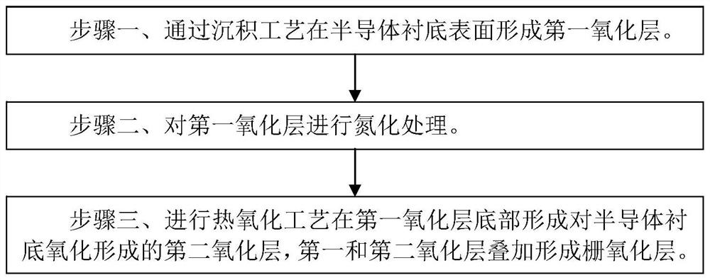
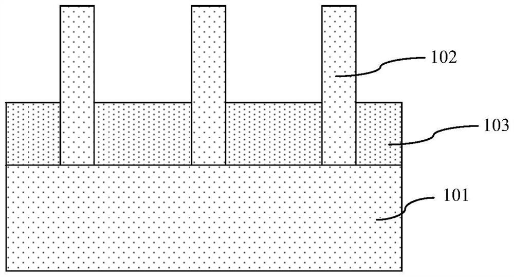
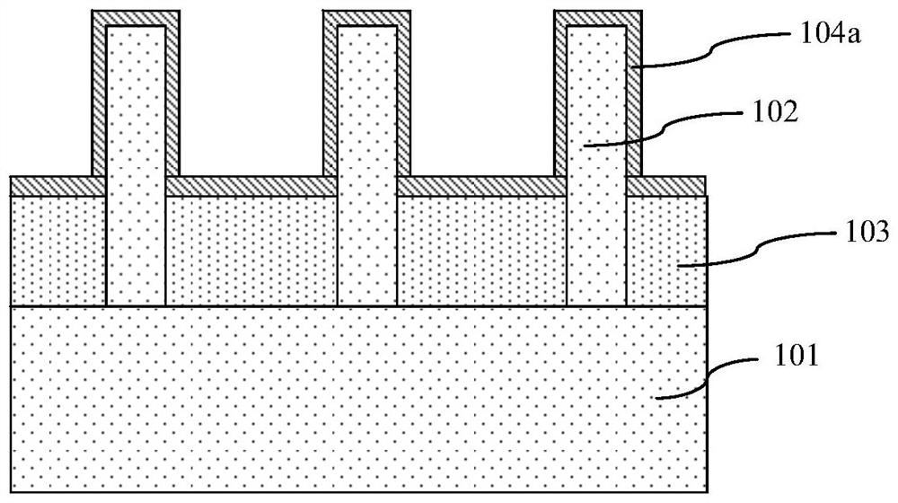
[0029] Such as figure 1 As shown, it is a flow chart of the method for manufacturing the gate oxide layer 104 according to the embodiment of the present invention; Figure 2A to Figure 2E Shown is a schematic diagram of the device structure in each step of the method for manufacturing the gate oxide layer 104 according to the embodiment of the present invention; the method for manufacturing the gate oxide layer 104 according to the embodiment of the present invention includes the following steps:

[0030] Step 1, such as Figure 2A As shown, a semiconductor substrate 101 is provided.

[0031] In the embodiment of the present invention, the material of the semiconductor substrate 101 includes silicon.

[0032] A fin body 102 is formed on the semiconductor substrate 101 . The fin body 102 is formed by performing patterned etching on the semiconductor substrate 101 .

[0033] In a preferred embodiment, the patterned etching process includes: forming a hard mask layer on the t...


PUM


Abstract

The invention discloses a method for manufacturing a gate oxide layer. The method comprises the following steps of: 1, forming a first oxide layer on the surface of a semiconductor substrate through a deposition process; and 2, carrying out nitriding treatment on the first oxide layer. And 3, performing a thermal oxidation process to form a second oxide layer formed by oxidizing the semiconductor substrate at the bottom of the first oxide layer, and overlapping the first oxide layer and the second oxide layer to form a gate oxide layer. The method can reduce the loss of the semiconductor substrate under the condition of ensuring the electrical thickness and quality of the gate oxide layer, is especially suitable for reducing the loss of the fin body in the manufacturing of an input / output device of a fin-type transistor, and enables the critical size of the fin body to be maintained.

Description

technical field [0001] The invention relates to a method for manufacturing a semiconductor integrated circuit, in particular to a method for manufacturing a gate oxide layer. Background technique [0002] The gate dielectric layer in the fin transistor (FinFET) covers the top surface and side surfaces of the fin body (Fin). The fin body is usually formed by patterning a semiconductor substrate, and the semiconductor substrate is usually a silicon substrate, so the fin body is also usually a silicon fin body. [0003] A core (Core) device (device) and an input-output (IO) device are usually integrated on the same semiconductor substrate at the same time. The IO device withstands a higher voltage, and the size of the device will also be larger, and the gate dielectric layer usually uses a gate oxide layer. In the existing method, the gate oxide layer is formed by performing thermal oxidation on the fin body, and the thermal oxidation process can adopt an in-situ stream gener...

Claims


Application Information

Patent Timeline
Patent Type & Authority Applications(China)
IPC IPC(8): H01L21/28H01L21/336H01L21/762H01L29/78
CPCH01L29/785H01L29/66795H01L21/28158H01L21/76224
Inventor 李勇
Owner SHANGHAI HUALI INTEGRATED CIRCUTE MFG CO LTD
Why Eureka
Try Eureka