Preparation method of avalanche photodetector

An avalanche photoelectric and detector technology, applied in the field of photoelectric detectors, can solve the problems of inconsistency of detectors, difficult diffusion of Zn, and reduced yield, etc., and achieves reduction of tunneling dark current, high crystal quality, and reduction of electric field strength. Effect

Pending Publication Date: 2022-03-01
北京英孚瑞半导体科技有限公司
View PDF0 Cites 1 Cited by
  • Summary
  • Abstract
  • Description
  • Claims
  • Application Information

AI Technical Summary

Problems solved by technology

However, Zn diffusion is a difficult and highly variable process to precisely control
Instability of the Zn diffusion process causes detector inconsistencies while reducing yield in production

Method used


Image

  • Preparation method of avalanche photodetector
  • Preparation method of avalanche photodetector
  • Preparation method of avalanche photodetector

Examples


Embodiment Construction

[0051] In order to enable those skilled in the art to better understand the solution of the present invention, the technical solution of the present invention will be further described below in conjunction with specific examples.

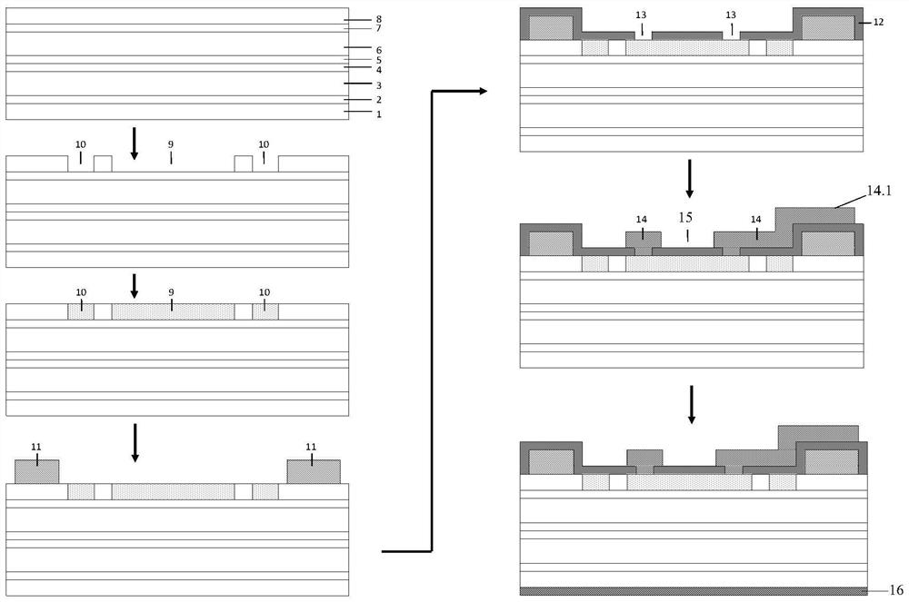
[0052] Such as figure 1 Shown, a kind of preparation method of avalanche photodetector comprises the following steps:

[0053] Step 1: On the p-type InP substrate 1, grow the p-type InP buffer layer 2, InP 0.53 Ga 0.47 As absorption layer 3, In 1-x-y Al x Ga y As bandwidth gradient layer 4, p-type In 0.52 Al 0.48 As charge control layer 5, In 0.52 Al 0.48 As multiplication layer 6, In x Ga 1-x As y P 1-y The stop layer 7 and the p-type InP capping layer 8 are etched.

[0054] Step 2: Using SiO 2 The patterned hard mask uses an etching method to etch the p-type InP cap layer 8 in a specific area. The etched area includes a central area and one or more annular areas surrounding the central area. In this embodiment, it includes An annula...


PUM

PropertyMeasurementUnit
Thicknessaaaaaaaaaa
Thicknessaaaaaaaaaa
Doping concentrationaaaaaaaaaa

Abstract

The invention discloses a preparation method of an avalanche photodetector. The preparation method comprises the following steps: firstly, sequentially growing a p-type InP buffer layer, an In < 0.53 > Ga < 0.47 > As absorption layer, an In < 1-x-y > Al < x > Ga < y > As bandwidth gradient layer, a p-type In < 0.52 > Al < 0.48 > As charge control layer, an In < 0.52 > Al < 0.48 > As multiplication layer, an In < x > Ga < 1-x > As < y > P < 1-y > corrosion cut-off layer and a p-type InP cover layer on a p-type InP substrate; then corroding the p-type InP cover layer, wherein the corroded region comprises a central region and one or more annular regions surrounding the central region; carrying out secondary epitaxy on n-type InP in the corroded region to form an n-type InP central collector region and an n-type InP electric field protection ring; then depositing a SiO2 layer, and etching off SiO2 in a partial region to form a circle of annular SiO2 isolation layer; depositing an optical anti-reflection film and forming a metal contact window on the optical anti-reflection film above the central collector region; then constructing an upper electrode, wherein the upper electrode is in contact with the central collector region through the metal contact window; and finally, preparing a back electrode on the back surface of the InP substrate.

Description

technical field [0001] The invention belongs to the technical field of photodetectors, and in particular relates to a preparation method of an avalanche photodetector. Background technique [0002] The working principle of the avalanche photodetector is to use the p-i-n junction under a relatively high reverse bias electric field. Photons are incident on the i region to make electrons transition from the valence band to the conduction band, forming electron-hole pairs. Under the action of a strong electric field, the electrons- The hole pairs get accelerated, collide with other atoms, create additional electron-hole pairs and keep on happening. Since the incidence of fewer photons or even a single photon can trigger the avalanche multiplication process and cause changes in the macroscopic current, the avalanche photodetector has extremely high sensitivity and detection efficiency, and has a very high potential in the field of weak light detection or even single photon detect...

Claims


Application Information

Patent Timeline
IPC IPC(8): H01L31/18H01L31/107
CPCH01L31/1844H01L31/1075Y02P70/50
Inventor 杨志茂王斌
Owner 北京英孚瑞半导体科技有限公司
Why Eureka
Try Eureka