Method for calibrating incident energy density of front surface of wafer

A technology of incident energy and energy density, used in laser welding equipment, electrical components, circuits, etc., can solve the problems of low activation efficiency of sub-melt nanoscale, limited selection of ultra-high-speed pyrometers, and unreliability.

Pending Publication Date: 2022-03-04
SHANGHAI HUALI MICROELECTRONICS CORP
View PDF0 Cites 0 Cited by
  • Summary
  • Abstract
  • Description
  • Claims
  • Application Information

AI Technical Summary

Problems solved by technology

[0007] The present invention is aimed at the limited selection of ultra-high-speed pyrometers in the traditional LSA in the prior art, and the large temperature change rate caused by the optical and thermal characteristics related to the layout, which brings some challenges to shortening the annealing time,

Method used


Image

  • Method for calibrating incident energy density of front surface of wafer
  • Method for calibrating incident energy density of front surface of wafer
  • Method for calibrating incident energy density of front surface of wafer

Examples


Embodiment Construction

[0035] In order to illustrate the technical content, structural features, achieved goals and effects of the present invention in detail, the following will be described in detail in conjunction with the embodiments and accompanying drawings.

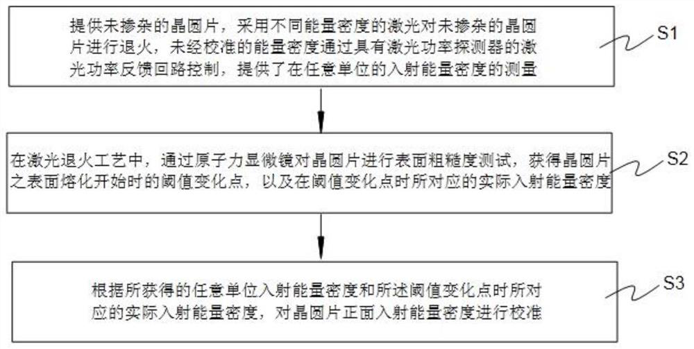
[0036] see figure 1 , figure 1 Shown is a flow chart of the method for calibrating the front incident energy density of the wafer according to the present invention. The method for calibrating the front incident energy density of the wafer includes:

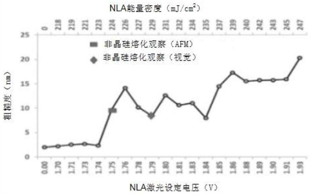
[0037] Executing step S1: providing an undoped wafer c-Si (100), using lasers with different energy densities to perform laser annealing on the undoped wafer, the uncalibrated energy density (ED) is obtained by having Laser power feedback loop control of the laser power detector, providing measurement of incident energy density in arbitrary units;

[0038] Execute step S2: in the laser annealing process, conduct a surface roughness test on the wafer through an atomic force microscope (AF...


PUM


Abstract

The invention relates to a method for calibrating the incident energy density of the front surface of a wafer, which comprises the following steps of: providing an undoped wafer, annealing by adopting laser with different energy densities, controlling the uncalibrated energy density by a feedback loop, and providing the measurement of the incident energy density in any unit; in the annealing process, surface roughness testing is conducted on a wafer through an AFM, and a threshold value change point at the beginning of surface melting and the corresponding actual incident energy density are obtained; and according to the incident energy density of any unit and the actual incident energy density corresponding to the threshold value change point, incident energy density calibration is carried out. According to the method, the incident laser pulse energy density is calibrated by using the sudden threshold change of the surface roughness measured by the AFM at the beginning of wafer surface melting; performing incident ED period monitoring on sub-melt boron doping activation of the silicon substrate at the temperature of 1300 DEG C; tool and process matching is performed using epitaxial regrowth of an amorphous doped silicon phosphorus layer at 1200 DEG C or below, and the matching is in the range of 1% of the energy density.

Description

technical field [0001] The invention relates to the technical field of semiconductor manufacturing, in particular to a method for calibrating the front incident energy density of a wafer. Background technique [0002] Millisecond laser pulse annealing (mSec, LSA) is adopted by many CMOS manufacturing equipment for dopant activation and gate reliability. The process uses a 10kHz fast pyrometer to measure the surface temperature of the wafer, which suppresses large differences in surface temperature. It is well known that annealing at high temperature is often required in order to activate dopant atoms and repair the damage caused by ion implantation. At the same time, the thermal budget of the annealing process must be small to reduce the transient enhanced diffusion effect (Transient-Enhance Diffusion, TED) of dopant atoms in the silicon device during the activation process, thereby protecting the structure of the abrupt junction, thereby effectively Control short channel ...

Claims


Application Information

Patent Timeline
IPC IPC(8): H01L21/268H01L21/324H01L21/67B23K26/02
CPCH01L21/324H01L21/268B23K26/02H01L21/67253
Inventor 周璇陆叶涛
Owner SHANGHAI HUALI MICROELECTRONICS CORP
Why Eureka
Try Eureka