Formation method of semiconductor device

A semiconductor and device technology, which is applied in the field of semiconductor device formation, can solve the problems such as the electrical performance of GAA structure MOSFET needs to be improved, and achieve the effect of improving the quality of formation, improving quality and reducing residue

Pending Publication Date: 2022-03-08
SEMICON MFG INT (SHANGHAI) CORP +1
View PDF0 Cites 0 Cited by
  • Summary
  • Abstract
  • Description
  • Claims
  • Application Information

AI Technical Summary

Problems solved by technology

[0005] However, in the prior art, the electrical performance of the GAA structure MOSFET still needs to be improved

Method used


Image

  • Formation method of semiconductor device
  • Formation method of semiconductor device
  • Formation method of semiconductor device

Examples


Embodiment Construction

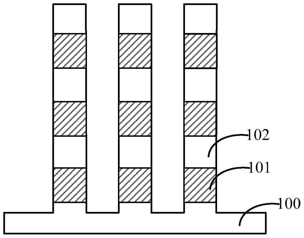
[0021] As the size of semiconductor devices shrinks, the pitch between fins becomes smaller and smaller, but as the pitch between fins gets smaller, there are some gaps in the process of forming the GAA structure MOSFET. Difficulty, please refer to the specific process Figure 1 to Figure 3 .

[0022] Figure 1 to Figure 3 It is a structural schematic diagram of the formation process of a semiconductor device.

[0023] refer to figure 1 , providing a substrate 100, forming a number of discretely arranged initial fins on the substrate 100, the initial fins including sacrificial layers 101 and channel layers 102 alternately stacked along the normal direction of the surface of the substrate 100 , the channel layer 102 is located between two adjacent sacrificial layers 101 and on the top sacrificial layer 101 .

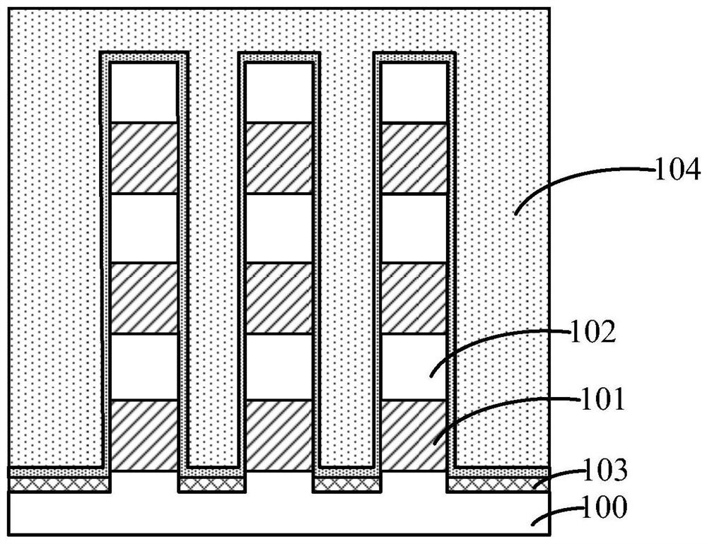
[0024] refer to figure 2 , forming an isolation structure 103 on the substrate 100, the isolation structure 103 covering part of the sidewalls of the initial fins, f...


PUM


Abstract

The invention relates to a semiconductor device forming method, which comprises the steps of providing a substrate, and forming a plurality of initial fin parts which are separately arranged on the substrate; forming an isolation structure on the substrate; forming connecting layers on the side walls of the initial fin parts and between the adjacent initial fin parts; forming a dummy gate structure crossing the initial fin part and the connecting layer on the substrate, wherein the dummy gate structure covers the side wall of the connecting layer and part of the top surface of the initial fin part; forming grooves in the initial fin parts at the two sides of the dummy gate structures, and forming source-drain doping layers in the grooves; a dielectric layer is formed on the substrate, the dielectric layer covers the dummy gate structure and the source-drain doped layer, and the top surface of the dielectric layer is flush with the top surface of the dummy gate structure; removing the dummy gate structure to form a gate structure; according to the invention, the quality of the finally formed semiconductor device can be improved.

Description

technical field [0001] The invention relates to the technical field of semiconductor manufacturing, in particular to a method for forming a semiconductor device. Background technique [0002] Metal-oxide-semiconductor field-effect transistor (MOSFET) is one of the most important elements in the modern integrated circuit, and the basic structure of MOSFET comprises: semiconductor substrate; Be positioned at the gate structure of semiconductor substrate surface, described gate structure comprises : a gate dielectric layer on the surface of the semiconductor substrate and a gate electrode layer on the surface of the gate dielectric layer; source and drain doped regions in the semiconductor substrate on both sides of the gate structure. [0003] With the development of semiconductor technology, the traditional planar MOSFET's ability to control the channel current becomes weaker, resulting in serious leakage current. Fin Field Effect Transistor (Fin FET) is an emerging multi-ga...

Claims


Application Information

Patent Timeline
Patent Type & Authority Applications(China)
IPC IPC(8): H01L21/336H01L29/78
CPCH01L29/66803H01L29/785H01L29/66606H01L29/66545H01L29/7848H01L29/165H01L29/78696H01L29/0673H01L29/66439H01L29/775B82Y10/00H01L29/42392H01L21/823437H01L29/66795H01L27/0886H01L21/823431H01L21/823481H01L29/0649H01L21/67075H01L21/823412H01L29/7851H01L21/823418
Inventor 王楠
Owner SEMICON MFG INT (SHANGHAI) CORP
Why Eureka
Try Eureka