Temperature optimization design method and system for reducing buckling deformation of PCB after lamination

A technology for optimizing design and warping, applied in CAD circuit design, design optimization/simulation, computer-aided design, etc., can solve the problems of increased thickness and weight, lack of versatility, and affecting PCB production efficiency, etc., to reduce warping deformation effect

Active Publication Date: 2022-03-15
SHANDONG UNIV
View PDF4 Cites 2 Cited by
  • Summary
  • Abstract
  • Description
  • Claims
  • Application Information

AI Technical Summary

Problems solved by technology

However, this method of adding extra copper and increasing the thickness of the insulating layer has two disadvantages: one is that the method is not universal, and for different PCBs, the amount and location of copper addition are ever-changing, which seriously affects the production efficiency of PCB; It will increase the overall thickness and weight of the PCB, which does not conform to the development trend of miniaturization and portability of electronic products

Method used


Image

  • Temperature optimization design method and system for reducing buckling deformation of PCB after lamination
  • Temperature optimization design method and system for reducing buckling deformation of PCB after lamination
  • Temperature optimization design method and system for reducing buckling deformation of PCB after lamination

Examples


Embodiment 1

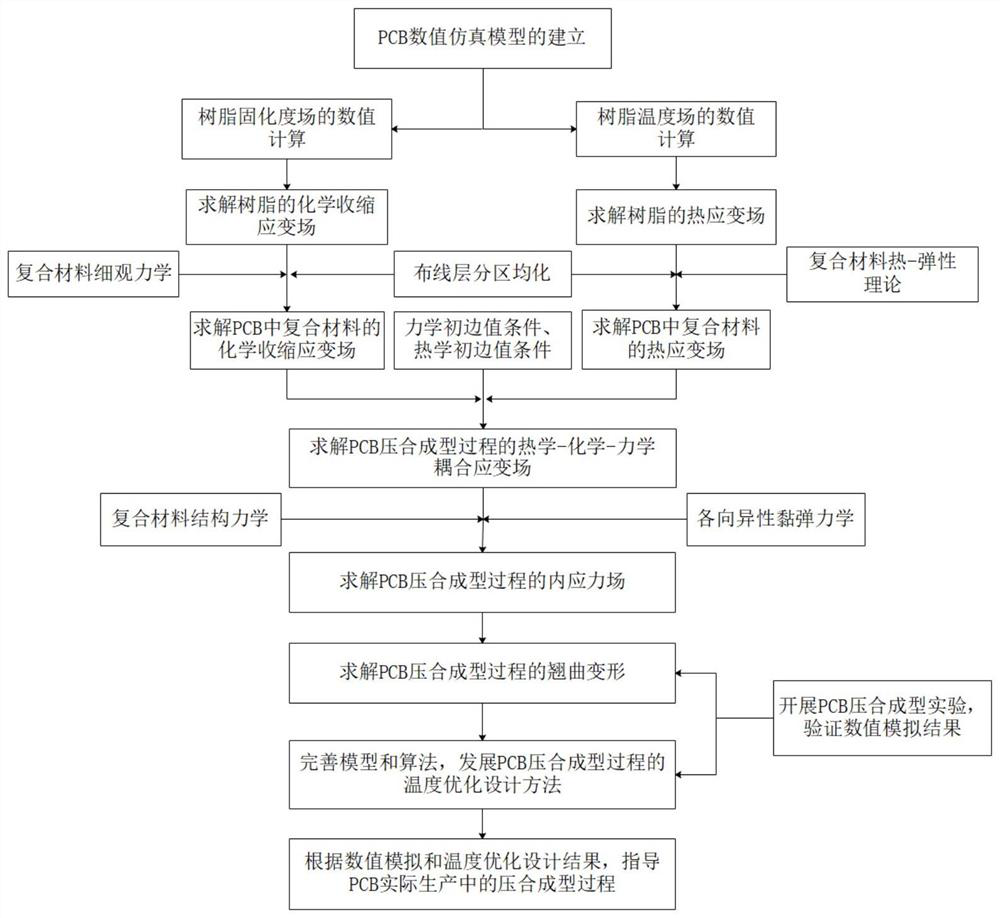
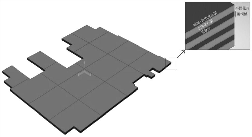
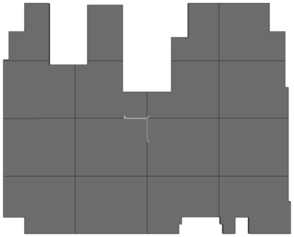
[0043] In one or more embodiments, a temperature optimization design method for reducing warpage deformation after PCB lamination is disclosed, using layered, partitioned modeling and thermal-chemical-mechanical coupling methods to simulate the PCB lamination process, Reveal the solidification deformation and residual stress formation mechanism of PCB during thermal compression-cold compression-opening and cooling to room temperature, and establish a thermal conduction-curing model of composite materials including thermal curing reaction, thermoelastic effect and physical and mechanical properties evolution of fiber composite materials , systematically and comprehensively analyze the size and regularity of the warping deformation change of the PCB during the pressing process, and form a prediction method for the curing deformation and residual stress of the PCB during the pressing process, and then can target various PCB specific pressing molding processes process, quickly and ...

Embodiment 2

[0085] In one or more embodiments, a temperature-optimized design system for reducing warpage after PCB lamination is disclosed, including:

[0086] Model building blocks for layered modeling of PCBs, partitioning mixed layers, and defining equivalent material performance parameters in each region;

[0087] Numerical simulation module, the numerical simulation module includes three parts: heat transfer analysis unit, strain field calculation unit and stress field calculation unit;

[0088] The heat transfer analysis unit is used for heat transfer analysis of the PCB pressing process, calculating the temperature field and curing degree field of the resin in the PCB; determining the maximum curing temperature of the PCB hot pressing stage;

[0089] The strain field calculation unit is used to calculate the thermal strain field and chemical shrinkage strain field of the resin in the PCB based on the temperature field and the curing degree field; and then obtain the thermal strain...

Embodiment 3

[0094] In one or more embodiments, a terminal device is disclosed, including a server, the server includes a memory, a processor, and a computer program stored on the memory and operable on the processor, and the processor executes the The program realizes the temperature optimization design method of reducing the warping deformation of the PCB after lamination in the first embodiment. For the sake of brevity, details are not repeated here.

[0095] It should be understood that in this embodiment, the processor can be a central processing unit CPU, and the processor can also be other general-purpose processors, digital signal processors DSP, application specific integrated circuits ASIC, off-the-shelf programmable gate array FPGA or other programmable logic devices , discrete gate or transistor logic devices, discrete hardware components, etc. A general-purpose processor may be a microprocessor, or the processor may be any conventional processor, or the like.

[0096] The me...


PUM


Abstract

The invention discloses a temperature optimization design method and system for reducing buckling deformation of a PCB after lamination, and the method comprises the steps: carrying out the layering modeling of the PCB, carrying out the partitioning of a mixed layer, and defining an equivalent material performance parameter in each region; calculating a temperature field and a curing degree field of resin in the PCB; determining the highest curing temperature of the PCB in the thermocompression bonding stage; obtaining a thermal strain field and a chemical shrinkage strain field of the composite material in the PCB based on the temperature field and the curing degree field; numerical simulation of PCB press-fit forming is carried out, and the buckling deformation amount of the PCB at the highest curing temperature is obtained; and changing the maximum curing temperature of the PCB in the press-fit forming numerical simulation process to obtain the buckling deformation of the PCB after press-fit forming at different maximum curing temperatures, and finally selecting the maximum curing temperature which enables the buckling deformation to be minimum. According to the invention, the problem caused by reducing the buckling deformation in the PCB press-fit forming process in the prior art is solved.

Description

technical field [0001] The invention relates to the technical field of reducing warpage deformation after PCB lamination, and in particular to a temperature optimization design method and system for reducing warpage deformation of PCB after lamination. Background technique [0002] The statements in this section merely provide background information related to the present invention and do not necessarily constitute prior art. [0003] Printed Circuit Board (PCB for short) is the carrier for electrical connection between electronic components and one of the most important components in the integrated circuit industry. The PCB is composed of the PCB itself and various components mounted on the surface. The PCB itself (also known as a bare board) can be divided into a single-layer board and a multi-layer board. In terms of manufacturing cost, when the PCB area is the same, the cost of multi-layer circuit boards is higher than that of single-layer and double-layer circuit board...

Claims


Application Information

Patent Timeline
Patent Type & Authority Applications(China)
IPC IPC(8): H05K3/00H05K3/46H05K1/02G06F30/20
CPCH05K3/0005H05K3/4638H05K1/0271G06F30/20G06F2115/12G06F2119/08
Inventor 张通贾玉玺黄斌程梦萱万国顺赵志彦郑瑞乾盛男
Owner SHANDONG UNIV
Why Eureka
Try Eureka