Electrostatic chuck and preparation method thereof
An electrostatic chuck and base technology, which is applied in the manufacture of circuits, electrical components, semiconductors/solid-state devices, etc., can solve problems that affect the stability of the chip plasma process, reduce the yield of chip products, and particle pollution, and achieve improved chip performance. Product yield, reduction of probability and risk, and improvement of stability
- Summary
- Abstract
- Description
- Claims
- Application Information
AI Technical Summary
Problems solved by technology
Method used
Image

Examples
no. 1 example
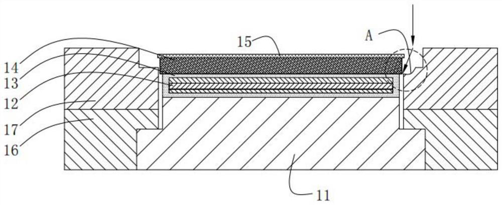
[0042] see figure 2, the electrostatic chuck provided in this embodiment includes a base 11, a heating layer 12 arranged on the base 11 for heating the wafer 15, and a heating layer 12 arranged on the heating layer 12 for absorbing the wafer 15. Adsorption layer 14, wherein, the base 11 is usually made of metal materials such as aluminum alloy, optionally, a radio frequency feed-in (not shown) is set in the base 11, which is used for electrical connection with the radio frequency power supply , to be able to feed in RF power. The heating layer 12 includes, for example, a heat insulating plate (or heat insulating layer), a heating plate (or heater) and a heat uniform plate (or heat uniform layer) arranged in sequence from bottom to top. Of course, in practical applications, the heating layer The specific structure of 12 is not limited thereto, as long as the wafer 15 can be heated. The adsorption layer 14 is generally made of insulating materials such as ceramics, and an ads...
no. 2 example
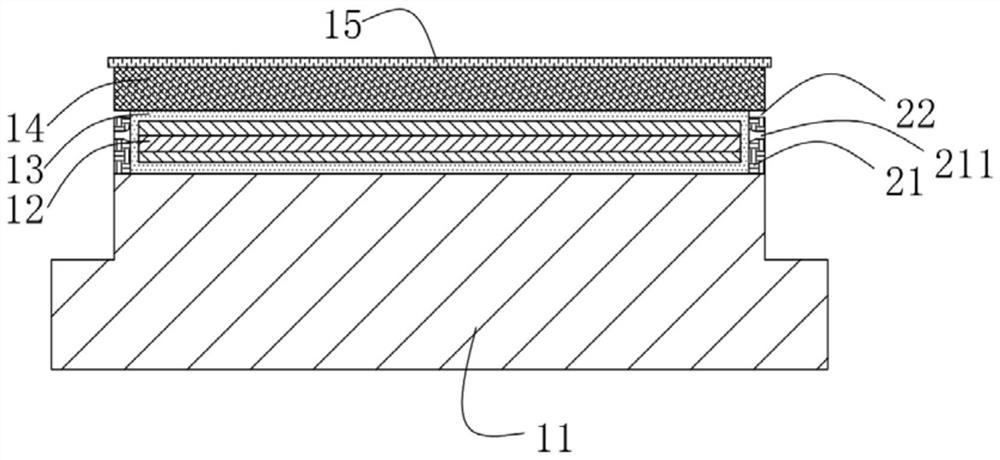
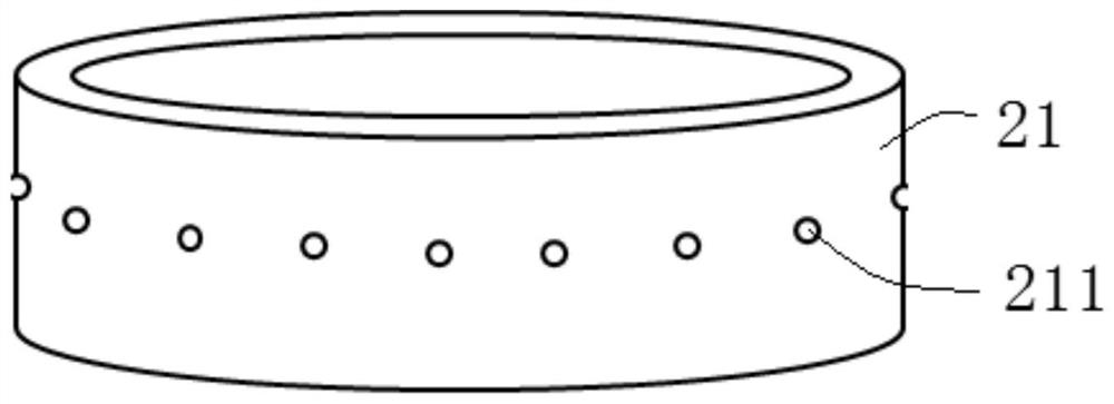
[0064] The electrostatic chuck provided in this embodiment is an improvement made on the basis of the above-mentioned first embodiment, specifically, as Figure 4 As shown, the electrostatic chuck also includes a protection ring 23 made of corrosion-resistant material, the protection ring 23 is arranged on the base 11, and surrounds the seal ring 21, and the protection ring 23 covers the side of the seal ring 21, absorbs The sides of the layer 14 and at least part of the sides of the base 11 . Specifically, the base 11 has a boss, and the protection ring 23 sequentially covers the side of the boss of the base 11 , the side of the sealing ring 21 and the side of the adsorption layer 14 from bottom to top. By means of the above-mentioned protective ring 23 , in combination with the sealing ring 21 , possible particle contamination due to the adhesive layer on the sides of the heating layer 12 can be completely eliminated.
[0065] In some optional embodiments, the corrosion-res...
no. 3 example
[0070] The electrostatic chuck provided in this embodiment is an improvement made on the basis of one of the above-mentioned first and second embodiments, specifically, as Figure 5 As shown, the edge region 111 of the base 11 for carrying the sealing ring 21' is lower than the central region 112 of the base 11 for carrying the heating layer 12.
[0071] The above-mentioned edge area 111 and central area 112 form an annular step, which not only facilitates the installation and positioning of the sealing ring 21', but also increases the axial height relative to the sealing ring 21 in the previous embodiment, and the increase in size is beneficial to Machining and installation of sealing rings.
PUM
| Property | Measurement | Unit |
|---|---|---|
| Opening diameter | aaaaa | aaaaa |
| Opening diameter | aaaaa | aaaaa |
| Thickness | aaaaa | aaaaa |
Abstract
Description
Claims
Application Information
 - R&D
- Intellectual Property
- Life Sciences
- Materials
- Tech Scout
- Unparalleled Data Quality
- Higher Quality Content
- 60% Fewer Hallucinations
Browse by: Latest US Patents, China's latest patents, Technical Efficacy Thesaurus, Application Domain, Technology Topic, Popular Technical Reports.
© 2025 PatSnap. All rights reserved.Legal|Privacy policy|Modern Slavery Act Transparency Statement|Sitemap|About US| Contact US: help@patsnap.com