Strip-shaped composite substrate for LED epitaxy and preparation method and preparation device of strip-shaped composite substrate
A composite substrate and strip-shaped technology, which is applied in the direction of electrical components, circuits, semiconductor devices, etc., can solve the problems of poor wavelength concentration, achieve the effect of improving crystallinity, good LED wavelength concentration, and improving product yield
- Summary
- Abstract
- Description
- Claims
- Application Information
AI Technical Summary
Problems solved by technology
Method used
Image
Examples
Embodiment 1
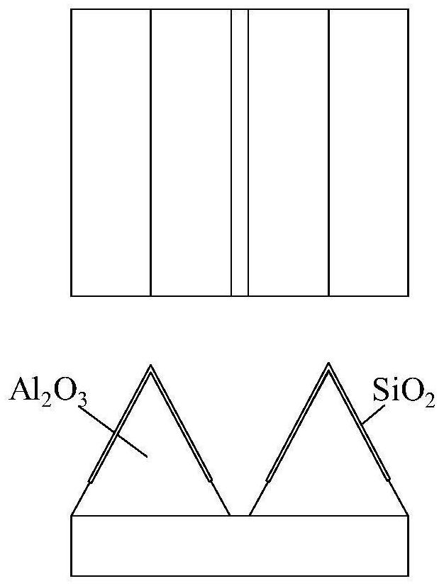
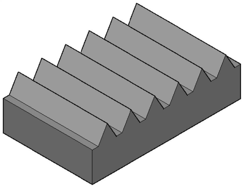
[0042] refer to Figure 2-3 , a strip-shaped composite substrate for LED epitaxy, the substrate is a sapphire substrate, the graphics on the sapphire substrate are strip-shaped, and several of the graphics are arranged periodically, and between two adjacent graphics There are intervals; the orientation of each of the patterns is consistent; the width of the bottom of the pattern is greater than the width of the top; the material of the pattern is Al 2 o 3 , the pattern side is covered with several layers of SiO 2 layer, the sapphire substrate has no pattern area without SiO 2 layer.
[0043] The number of GaN epitaxial grain boundaries grown on the strip-shaped sapphire substrate is less, which can significantly improve the crystallinity of the epitaxial layer and improve IQE, thereby improving the luminous efficiency of the LED.
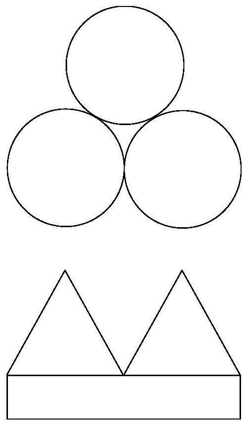
[0044] Traditional conical figures cannot emit polarized light, refer to figure 1 , and the strip substrate can obtain polarized light due to ...
Embodiment 2
[0048] A strip-shaped composite substrate for LED epitaxy. On the basis of Embodiment 1, the shapes of the figures are the same, the figures are horizontal triangular prisms, and the SiO 2 layer covering the graphic sidewalls.
[0049] The orientations of each of the figures are consistent when they are periodically arranged, that is, the long sides of the strip figures are parallel to each other, and the figures are horizontal triangular prisms. At this time, the angle between the incident light and each figure and each position is the same, By controlling the angle between the incident light and the pattern so that when it reaches the Brewster angle, the reflected light is completely polarized light, and by adjusting the polarization direction of the completely polarized light to be consistent with the vertical polarization mode, the amount of light passing through the vertical polarization mode is increased. .
[0050] the second part
Embodiment 3
[0052] refer to Figure 5 , a method for preparing a strip-shaped composite substrate for LED epitaxy, for preparing any strip-shaped composite substrate for LED epitaxy described in the first part, comprising the following steps
[0053] Vacuum-evaporating a layer of metal film on the sapphire substrate and the pattern;
[0054] Spin-coating a layer of photoresist on the sapphire substrate, the thickness of the photoresist is 2 μm-2.5 μm;
[0055] Reduce photoresist thickness to 150-500nm;
[0056] removing the metal film over the photoresist;
[0057] Multilayer SiO was grown on the pattern using magnetron sputtering 2 layer, each layer thickness 20nm; several SiO 2 the total thickness of the layers is less than the metal film thickness;
[0058] Use solvents and solutions to remove remaining photoresist and metal film.
[0059] The traditional composite substrate preparation method is to deposit a layer of low refractive index material on the surface of sapphire first...
PUM
| Property | Measurement | Unit |
|---|---|---|
| Thickness | aaaaa | aaaaa |
| Thickness | aaaaa | aaaaa |
| Thickness | aaaaa | aaaaa |
Abstract
Description
Claims
Application Information


