Manufacturing process of PERC battery piece
A production process and cell technology, applied in the field of PERC cell production technology, can solve problems such as unfavorable cell production, unfavorable cell optical absorption, and reduced cell conversion efficiency.
- Summary
- Abstract
- Description
- Claims
- Application Information
AI Technical Summary
Problems solved by technology
Method used
Image
Examples
Embodiment 1
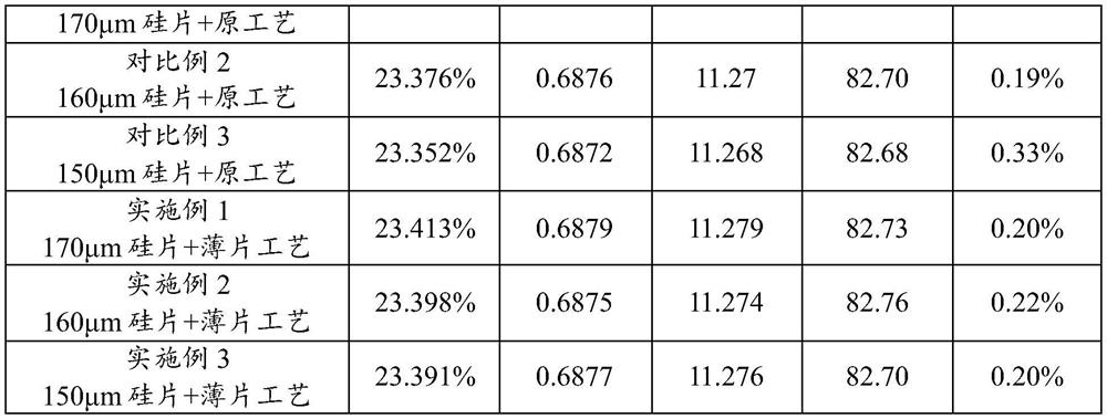
[0047] The embodiment of this application provides a PERC solar cell, which uses a single crystal P-type silicon wafer with a thickness of 170 μm as the silicon substrate, and is manufactured according to the following process:
[0048] (1) Texturing: Clean the P-type silicon wafer, and at the same time use KOH to perform texturing on the front side of the P-type silicon wafer to form a pyramid textured surface with a height of 2 μm.
[0049] (2) Diffusion: The P-type silicon wafer after texturing is placed in a diffusion furnace, and diffused for 40 minutes at a diffusion temperature of 800 ° C, so that phosphorus oxychloride is deposited on the front side of the P-type silicon wafer and thermally diffused. A phosphorus-doped N+ emitter junction layer with a thickness of 0.3 μm is obtained to form a PN junction.
[0050] (3) SE laser doping: the selective emitter is on the lightly doped P-type silicon wafer, and the doping and diffusion of the local area is carried out on the...
Embodiment 2
[0060] This embodiment provides a PERC solar cell, which uses a single crystal P-type silicon wafer with a thickness of 160 μm as a silicon substrate, and the rest of the manufacturing process is the same as that of Embodiment 1.
Embodiment 3
[0062] This embodiment provides a PERC solar cell, which uses a single crystal P-type silicon wafer with a thickness of 150 μm as a silicon substrate, and the rest of the manufacturing process is the same as that of Embodiment 1.
PUM
| Property | Measurement | Unit |
|---|---|---|
| thickness | aaaaa | aaaaa |
| thickness | aaaaa | aaaaa |
| height | aaaaa | aaaaa |
Abstract
Description
Claims
Application Information


