Growth method of large-size silicon carbide seed crystal and growth method of corresponding single crystal

A silicon carbide single crystal and silicon carbide seed technology, which is applied in the directions of single crystal growth, single crystal growth, crystal growth, etc., can solve the problems of low success rate, high process control and yield requirements, and large difference in seed crystal size. , to achieve the effect of low cost

Pending Publication Date: 2022-04-01
杭州乾晶半导体有限公司
View PDF4 Cites 0 Cited by
  • Summary
  • Abstract
  • Description
  • Claims
  • Application Information

AI Technical Summary

Problems solved by technology

The existing diameter expansion process has the following two problems: 1) The size of the seed crystal cannot be too different from the diameter of the crystal to be grown, otherwise polycrystalline defects are prone to appear at the edge of the expanded area
The entire diameter expansion process is complex, with many intermediate links, and high requirements for process control and yield of each link. Therefore, the success rate of "diameter expansion" growth is low, and silicon carbide single crystals of 8 inches and above are still difficult to obtain

Method used


Image

  • Growth method of large-size silicon carbide seed crystal and growth method of corresponding single crystal
  • Growth method of large-size silicon carbide seed crystal and growth method of corresponding single crystal
  • Growth method of large-size silicon carbide seed crystal and growth method of corresponding single crystal

Examples


Embodiment Construction

[0036] In order to facilitate the understanding of those skilled in the art, the present invention will be further described in detail below in conjunction with specific embodiments.

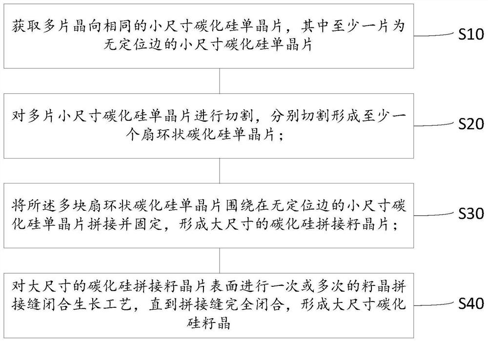
[0037] The embodiment of the present invention firstly provides a method for growing a large-sized silicon carbide seed crystal, please refer to figure 1 , including:

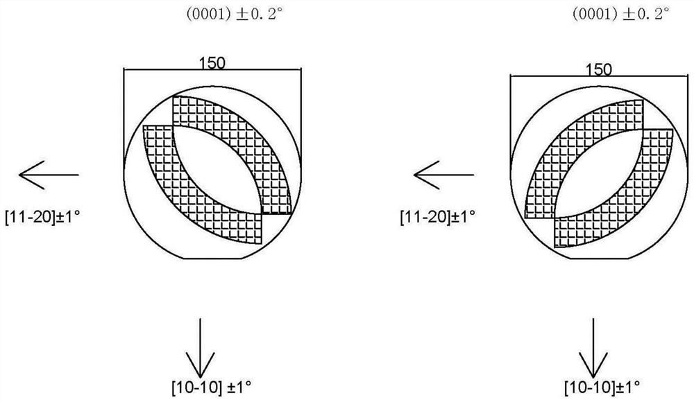
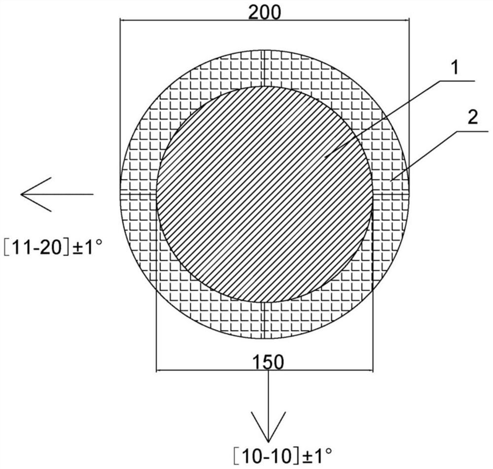
[0038] Step S10, obtaining a plurality of small-sized silicon carbide single wafers with the same crystal plane, at least one of which is a small-sized silicon carbide single wafer without positioning edges;

[0039] Step S20, cutting a plurality of small-sized silicon carbide single wafers along a specific crystal direction to form at least one sector-shaped silicon carbide single wafer, which is used to splice into a complete ring-shaped silicon carbide single wafer. Silicon single wafer, in which the inner diameter of the fan-shaped silicon carbide single wafer is consistent with the outer diameter of the small-sized silicon ...


PUM

PropertyMeasurementUnit
thicknessaaaaaaaaaa

Abstract

The invention relates to the field of silicon carbide crystal growth, and provides a growth method of a large-size silicon carbide seed crystal and a growth method of a large-size silicon carbide single crystal, which comprises the following steps of: cutting a plurality of small-size silicon carbide single crystal wafers with the same crystal faces along a specific crystal direction to form fan-shaped silicon carbide single crystal wafers; splicing and fixing the plurality of sector-ring-shaped silicon carbide single crystal wafers around the small-size silicon carbide single crystal wafer without the positioning edge according to the same spatial crystallization orientation to form a large-size silicon carbide spliced seed wafer, and carrying out a one-time or multi-time seed crystal splicing seam closed growth process until splicing seams are completely closed, so as to obtain the large-size silicon carbide spliced seed wafer. The problem that the large-size silicon carbide seed crystal cannot be obtained in the prior art is solved, and the cost is low.

Description

technical field [0001] The invention relates to the field of silicon carbide single crystal growth, in particular to a growth method of a large-size silicon carbide seed crystal and a corresponding single crystal growth method. Background technique [0002] As a representative of the third-generation semiconductor materials, silicon carbide (SiC) single crystal materials have superior properties such as large band gap, high breakdown electric field, high thermal conductivity, high electron saturation mobility and strong radiation resistance, which can meet the power requirements. The device's requirements for high temperature resistance, high power, and high voltage can also meet the requirements of radio frequency devices for harsh conditions such as high frequency and radiation resistance. [0003] Silicon carbide (SiC) single crystal materials are used in the field of semiconductor devices. Usually, single crystal materials are processed into thin wafers. A larger wafer s...

Claims


Application Information

Patent Timeline
Patent Type & Authority Applications(China)
IPC IPC(8): C30B29/36C30B23/00C30B33/06
Inventor 王明华朱鑫煌蒋琳张振远
Owner 杭州乾晶半导体有限公司
Why Eureka
Try Eureka