Medium-high temperature semiconductor thermoelectric conversion module based on thin film integrated crystal grains

A thermoelectric conversion and semiconductor technology, which is applied in the direction of thermoelectric devices that only use the Peltier or Seebeck effect, and the manufacture/processing of thermoelectric devices, can solve problems such as component deformation and stress, unusability, etc., to reduce defects and reduce loss , the effect of stable performance

Pending Publication Date: 2022-04-01
NUCLEAR POWER INSTITUTE OF CHINA
View PDF4 Cites 0 Cited by
  • Summary
  • Abstract
  • Description
  • Claims
  • Application Information

AI Technical Summary

Problems solved by technology

However, the application target of this device is a refrigeration system, and the design is based on the packaging principle of a semiconductor refrigeration module. The deformation and stress of each component during the high and low temperature conversion process are also not considered in the selection of components and structural design, so it cannot be used at a higher temperature ( Use at 300℃~500℃)

Method used


Image

  • Medium-high temperature semiconductor thermoelectric conversion module based on thin film integrated crystal grains

Examples


Embodiment 1

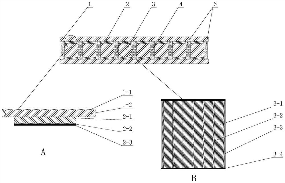
[0030] Please refer to figure 1 , this embodiment 1 is mainly composed of a heat-conducting substrate 1, a flow deflector 2, a thin-film integrated die 3, a die positioner 4, and a thermal insulation filling medium 5, etc.

[0031] Wherein the material of the outer elastic heat conduction layer 1-1 on the outside of the heat conduction substrate 1 is graphene or carbon nanotubes, preferably with a thickness of 10 microns; the material of the inner ceramic substrate 1-2 is aluminum nitride ceramics, alumina ceramics or silicon nitride ceramics , preferably aluminum nitride ceramics, the thickness is preferably 300 microns, and the external dimensions are preferably 60×60 mm;

[0032] The flow guide sheet 2 is located inside the heat conduction substrate 1, and consists of a metal substrate 2-1, an internal elastic heat conduction (flow) layer 2-2 and a metal deposition layer A2-3 from outside to inside. Wherein the metal substrate 2-1 material is copper, stainless steel, iron,...


PUM

PropertyMeasurementUnit
thicknessaaaaaaaaaa
thicknessaaaaaaaaaa
thicknessaaaaaaaaaa

Abstract

The invention discloses a semiconductor thermoelectric conversion module capable of realizing direct thermoelectric conversion by using a semiconductor under a medium-high temperature condition. The semiconductor thermoelectric conversion module structurally comprises a heat conduction substrate, a flow deflector, a thin film integrated crystal grain, a crystal grain locator, a heat insulation filling medium and the like. The requirements of thermoelectric conversion efficiency, effective temperature transfer, cold and hot impact resistance, medium and high temperature operation reliability and the like are met in material selection, structural design and processing technology of all parts. Practices prove that the semiconductor thermoelectric conversion module can realize high-efficiency thermoelectric direct conversion under medium and high temperature conditions, and can ensure stable operation in the process of greatly increasing and decreasing the temperature.

Description

technical field [0001] The invention relates to the technical field of semiconductor power generation, in particular to a medium-high temperature semiconductor thermoelectric conversion module based on thin film integrated grains. Background technique [0002] The semiconductor thermoelectric conversion module can realize static direct mutual conversion between heat energy and electric energy. In our modern life, a large amount of energy is consumed every day, ranging from industrial production, transportation, to daily life, but these energies have not been fully utilized. In the process of energy utilization, there is always a part of energy that cannot be utilized, but is converted into heat energy and lost. This part of energy can be utilized by performing thermoelectric conversion with semiconductor thermoelectric conversion modules. [0003] For example, a utility model (CN201584931U) discloses a low-temperature semiconductor power generation device that recovers was...

Claims


Application Information

Patent Timeline
Patent Type & Authority Applications(China)
IPC IPC(8): H01L35/32H01L35/30H01L35/34
Inventor 仇子铖袁德文闫晓孙桂铖张友佳徐建军乔红威
Owner NUCLEAR POWER INSTITUTE OF CHINA
Why Eureka
Try Eureka