Pier type structure for diode on-chip test and preparation method thereof

A diode and bridge pier type technology is applied in the field of "bridge pier type" structure and its preparation, which can solve the problems that affect the accuracy of extraction parameters and cannot be eliminated, and achieve the effects of perfecting diode modeling, improving differences and improving accuracy.

Pending Publication Date: 2022-04-05
NAT SPACE SCI CENT CAS
View PDF0 Cites 0 Cited by
  • Summary
  • Abstract
  • Description
  • Claims
  • Application Information

AI Technical Summary

Problems solved by technology

The extracted parasitic parameters of the Schottky diode thus obtained include the influence of a thicker substrate, which cannot be eliminated in subsequent data processing, which affects the accuracy of the extracted parameters

Method used


Image

  • Pier type structure for diode on-chip test and preparation method thereof
  • Pier type structure for diode on-chip test and preparation method thereof
  • Pier type structure for diode on-chip test and preparation method thereof

Examples


Embodiment Construction

[0034] The technical solutions provided by the present invention are further described below in conjunction with the examples.

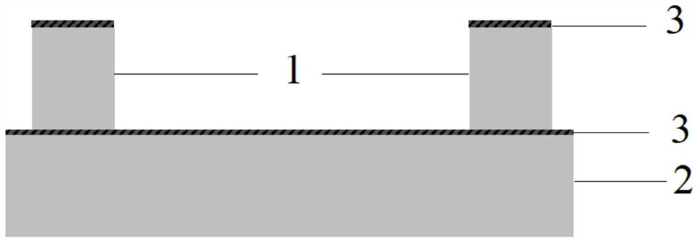
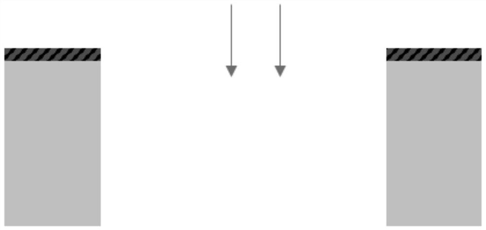
[0035] Such as figure 1 As shown, it is a schematic cross-sectional view of the "bridge pier" structure used for diode on-chip testing according to the present invention. The structure of the present invention includes: a "bridge pier" structure 1 arranged on a silicon gasket 2, and the "bridge pier" "Formula" structure 1 includes two pillars or platforms such as cuboids, which are used to support the monolithic circuit to be tested and bear the pressure of the probes during the test. There is a layer of photoresist 3 on the surface of the "bridge pier" structure 1. When assembling the monolithic circuit to be tested, an alignment structure is provided on the front side to realize the alignment between the monolithic circuit to be tested and the "bridge pier" structure 1. alignment, so that the monolithic circuit to be tested is assembled on the pho...


PUM

PropertyMeasurementUnit
heightaaaaaaaaaa
thicknessaaaaaaaaaa
thicknessaaaaaaaaaa

Abstract

The invention relates to a bridge pier type structure for diode on-chip test and a preparation method thereof, the structure comprises a bridge pier type structure arranged on a silicon gasket, and the bridge pier type structure comprises two column bodies or table bodies and is used for supporting a to-be-tested monolithic circuit and bearing the pressure of a probe during test. The method comprises the following steps: carrying out photoetching pattern definition on a silicon wafer according to the structure of a monolithic circuit to be tested, protecting the position of a'pier type 'structure by adopting photoresist, then carrying out deep silicon etching according to a photoetching pattern, and integrally etching through the silicon wafer with complete thickness to form the'pier type' structure; a complete silicon wafer is selected as a silicon gasket, a layer of photoresist is spin-coated on the silicon gasket to enable the silicon gasket to be stably connected with the bridge pier type structure, and after drying, a monolithic circuit is assembled on the surface of the etched silicon wafer through a cross alignment structure to form the bridge pier type structure for diode on-chip testing. According to the invention, the influence of the thickness of a single substrate on diode parasitic parameter extraction is improved.

Description

technical field [0001] The invention relates to the field of Schottky diode on-chip test substrate structure, in particular to a "bridge pier" structure for diode on-chip test and a preparation method thereof. Background technique [0002] Terahertz wave is an electromagnetic wave between microwave and millimeter wave and infrared light, its frequency range is usually between 0.1-10THz, and the corresponding wavelength is 0.03-3mm. Since the 1990s, with the development of laser technology and compound semiconductor technology, people's research on terahertz science has made great progress. The terahertz frequency domain is in the transition zone from the macroscopic classical theory to the microscopic quantum theory. Due to its special spectral position, the terahertz wave exhibits many excellent characteristics, including: it can penetrate most non-metallic materials, and will not cause material Molecular ionization is especially suitable for biological tissue detection an...

Claims


Application Information

Patent Timeline
Patent Type & Authority Applications(China)
IPC IPC(8): H01L23/544H01L21/027
Inventor 朱皓天刘锶钰张德海孟进
Owner NAT SPACE SCI CENT CAS
Why Eureka
Try Eureka