
A patch diode chip packaging device

A chip packaging and packaging device technology, applied in the direction of transportation and packaging, electrical components, conveyor objects, etc., can solve problems such as difficulty in coordination, affect processing efficiency, and complicated control, and achieve the effect of reducing difficulty

Active Publication Date: 2022-05-24
NANTONG GAOXIN SCI & TECH DEVCO
View PDF5 Cites 0 Cited by
  • Summary
  • Abstract
  • Description
  • Claims
  • Application Information

AI Technical Summary

Problems solved by technology

Through the setting of the core and jumping film mechanism along the lead frame conveying line, not only the step-by-step continuous conveying of the lead frame can be realized, but also the gluing, core sticking and core loading can be completed efficiently, and then the sticking and jumping can be completed during the transportation sheet, which greatly improves the process efficiency, but each step is operated separately, which affects the processing efficiency. Therefore, this equipment was invented for continuous operation, and the structure of feeding also requires more power components to control, control It is more complicated and difficult to coordinate

Method used


Image

  • A patch diode chip packaging device
  • A patch diode chip packaging device
  • A patch diode chip packaging device

Examples


Embodiment

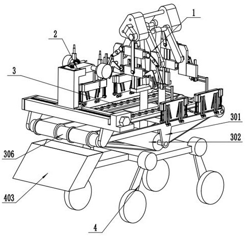
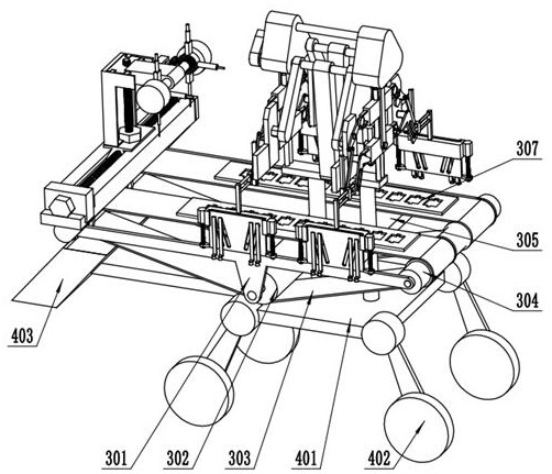
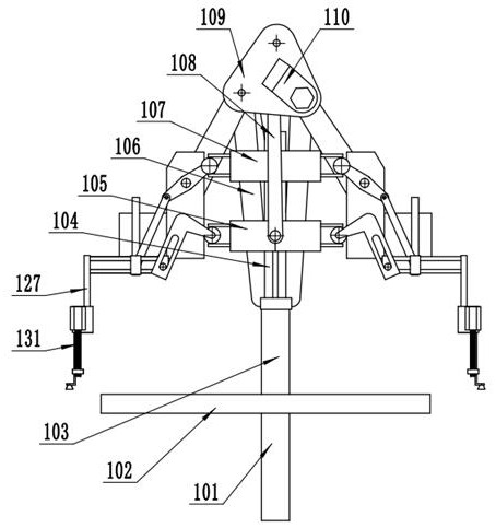
[0027] Example: as Figure 1-Figure 10 As shown, a SMD diode chip packaging device includes a conveying device 3, a feeding device 1 and a packaging device 2 are installed on the conveying device 3, a moving device 4 is installed under the conveying device 3, and the moving device 4 includes a chassis 401, and the bottom The lower end of the frame 401 is equipped with four wheels 402 for walking and moving; the feeding device 1 includes a pick-up assembly and two crank-slider mechanisms, and the output end of the first crank-slider mechanism is connected to control the vertical movement of the pick-up assembly. The vertical movement assembly, the output end of the second crank-slider mechanism is connected with a transverse movement assembly for controlling the lateral movement of the pickup assembly, the first ends of the two crank parts are fixedly connected at the same point, and the two cranks are not in the same straight line On the upper side, the two cranks are driven b...


PUM


Abstract

The invention discloses a patch diode chip packaging device, which relates to the field of semiconductor elements and includes a conveying device. The conveying device is equipped with a feeding device and a packaging device. The feeding device includes a pick-up assembly and two crank slider mechanisms. The output end of the first slider crank mechanism is connected with a vertical movement assembly for controlling the vertical movement of the pickup assembly, and the output end of the second slider crank mechanism is connected with a traverse assembly for controlling the lateral movement of the pickup assembly. The drive drives the two crank slider structures to realize the control of the pick-up assembly, so that the pick-up assembly can move sequentially according to the positional relationship of each device of the machine.

Description

technical field [0001] The invention relates to the field of semiconductor elements, in particular to a chip diode chip packaging device. Background technique [0002] The package form refers to a housing for mounting a semiconductor integrated circuit chip. It not only plays the role of mounting, fixing, sealing, protecting the chip and enhancing the electrical and thermal performance, but also connected to the pins of the package shell with wires through the contacts on the chip, and these pins pass through the wires on the printed circuit board. Connect with other devices, so as to realize the connection between the internal chip and the external circuit. On the one hand, the chip can be isolated from the outside world to prevent the corrosion of the chip circuit caused by the impurities in the air and cause the electrical performance to decline; on the other hand, the packaged chip is also easier to install and transport. The packaging process of ultra-thin SMD diodes ...

Claims


Application Information

Patent Timeline
Patent Type & Authority Patents(China)
IPC IPC(8): H01L21/677H01L21/67
Inventor 张晓林
Owner NANTONG GAOXIN SCI & TECH DEVCO
Features
  • Generate Ideas
  • Intellectual Property
  • Life Sciences
  • Materials
  • Tech Scout
  • Unparalleled Data Quality
  • Higher Quality Content
  • 60% Fewer Hallucinations
Learn More