Cavity type piezoelectric single crystal acoustic resonator and preparation method thereof
A piezoelectric single crystal and acoustic wave resonator technology, applied in the direction of electrical components, impedance networks, etc., can solve problems such as limitations, incompatibility, and etching process difficulties, and achieve the effects of avoiding crystal defects, stable mechanical properties, and reducing the difficulty of preparation
- Summary
- Abstract
- Description
- Claims
- Application Information
AI Technical Summary
Problems solved by technology
Method used
Image
Examples
Embodiment 1
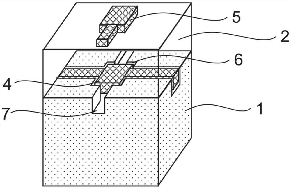
[0071] Example 1 see figure 1 A cavity-type piezoelectric single crystal acoustic resonator provided in this embodiment includes a wafer substrate 1 (ie, a wafer-level substrate, referred to as the substrate hereinafter) and a piezoelectric single crystal thin film 2 . The lower end surface (defined as the first surface) of the piezoelectric single crystal thin film is provided with a lower electrode film 4 (defined as the first electrode), and the upper end surface is provided with an upper electrode film 5 (defined as the second electrode). The lower end face of the piezoelectric single crystal thin film is bonded to the substrate surface, and the substrate surface forms exhaust channels 7 and air cavities 6 that cross each other vertically and horizontally. The air cavity 6 is located at the intersection node of the exhaust channels 7, and The exhaust channels 7 communicate with each other, the lower electrode film 4 is arranged in the corresponding air cavity 6, and the ex...
Embodiment 2
[0085] Embodiment 2 The structure of a cavity-type piezoelectric single crystal acoustic resonator provided in this embodiment is similar to that of Embodiment 1, except that a buffer layer 8 is formed on the substrate.
[0086] The preparation method of a cavity-type piezoelectric single crystal acoustic resonator in this embodiment is also similar to that of Embodiment 1, specifically including the following steps:
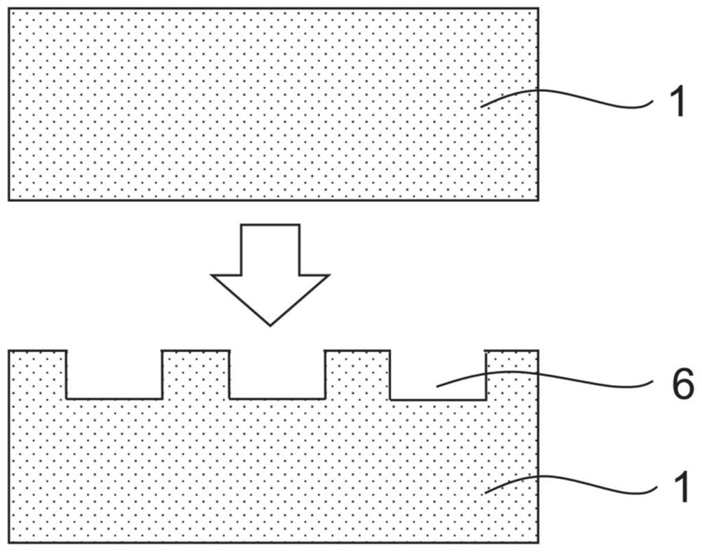
[0087] (1) Please refer to Figure 7, Obtain a 4-inch high-resistance (100) silicon wafer with a thickness of 500 μm, sequentially undergo ultrasonic cleaning with acetone, alcohol, deionized water, and alcohol, and then dry it with a nitrogen gun. A silicon dioxide layer was prepared as a buffer layer with a thickness of 300 nm by using a plasma enhanced chemical vapor deposition method. Using photolithography and etching technology to form a patterned wafer substrate, the specific steps are: first, perform photolithography process, including baking, coating a...
PUM
| Property | Measurement | Unit |
|---|---|---|
| thickness | aaaaa | aaaaa |
| thickness | aaaaa | aaaaa |
| thickness | aaaaa | aaaaa |
Abstract
Description
Claims
Application Information


