
Global layout method of clock-driven fpga chip based on multi-electric field model

A global layout, clock-driven technology, applied in electrical digital data processing, instrumentation, computing and other directions, can solve the problems affecting the quality of layout results, can not achieve good layout quality, poor results, etc., to achieve good computing efficiency and layout results quality effect

Active Publication Date: 2022-05-20
PEKING UNIV
View PDF4 Cites 0 Cited by
  • Summary
  • Abstract
  • Description
  • Claims
  • Application Information

AI Technical Summary

Problems solved by technology

[0006] (1) Existing FPGA layout tools do not work well on large-scale FPGA layout problems
The existing FPGA layout tools mainly use the global layout algorithm based on quadratic programming. However, with the continuous increase of chip size and chip complexity, the FPGA global layout algorithm based on quadratic programming cannot achieve very good results in large-scale FPGA layout problems. good layout quality
[0007] (2) Existing FPGA global layout algorithms seldom consider restrictions on clock signal routing in the global layout stage
Due to the lack of restrictions on clock signal routing in the layout stage, the position of some devices that violate the clock signal routing needs to be adjusted in the later legalization stage, which will affect the quality of the entire layout result
[0008] In summary, the existing traditional FPGA global layout algorithm is difficult to achieve good layout results on large-scale FPGA layout problems, and because the restrictions on clock signal routing are less considered in the global layout stage, the legalization in the later stage of layout Adjustment of devices in stages that violate clock routing signals can affect placement quality

Method used


Image

  • Global layout method of clock-driven fpga chip based on multi-electric field model
  • Global layout method of clock-driven fpga chip based on multi-electric field model
  • Global layout method of clock-driven fpga chip based on multi-electric field model

Examples


Embodiment Construction

[0028] The present invention is further described by example, but does not limit the scope of the present invention in any way.

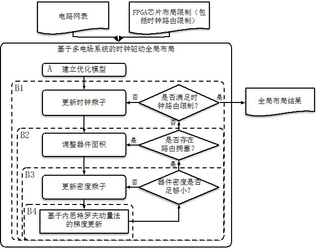
[0029] The present invention provides an efficient clock-driven FPGA global layout algorithm based on a multi-electric field system, the input includes a circuit netlist and FPGA chip layout limitations, the output takes into account the clock routing limitations of the FPGA global layout results.

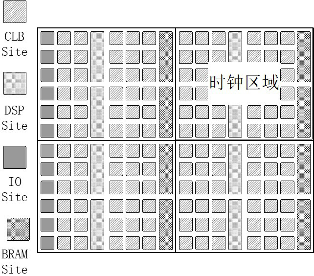
[0030] The following first provides a description of the input of the present invention. In the present invention, the circuit netlist is used represents, where Represents a collection of devices, Represents a collection of hyper-edges between devices. Note In FPGA layout issues, a hyper-edge Multiple devices can be connected at the same time. Each device has its own type, in this embodiment, the device may be typed as a look-uptable (Look-upTable, hereinafter referred to as LUT), flip-flop (Flip Flop, hereinafter referred to as FF), digital signal proce...


PUM


Abstract

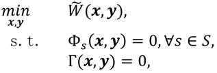
The invention discloses a clock-driven FPGA chip global layout method based on a multi-electric field model, which establishes an electric field model for the density distribution of a variety of different device types; the circuit netlist obtained after input logic synthesis and the layout restrictions of the FPGA chip make In the global layout stage, the layout results that are conducive to meeting the clock routing constraints in the legalization stage are generated; the constrained non-convex optimization model is converted into an unconstrained non-convex optimization model; the nested optimization framework method is used to solve the constraints uniformly, that is, the multi-electric field-based The model's clock drives the FPGA chip global layout. The method of the present invention also adopts an algorithm structure suitable for parallel computing by the GPU, which can make full use of the GPU for accelerated computing, thereby efficiently obtaining better layout results that meet clock routing constraints in the global layout stage, and improving the quality and effect of the global layout of the FPGA chip .

Description

Technical field [0001] The present invention belongs to the electronic design automation (Electronic Design Automation, hereinafter referred to as EDA) technical field, relates to the chip integrated circuit physical design for field programmable gate array (FieldProgrammable Gate Array, hereinafter referred to as FPGA) global layout technology, specifically relates to a clock-driven FPGA global layout method based on a multi-electric field model system. Background [0002] An FPGA is a semi-custom integrated circuit chip with programmable characteristics that is pre-designed on silicon wafers. In the FPGA chip manufacturing process, the manufacturer will design the programmable gate logic device on the silicon in advance; during the customer's use process, the designer can describe the customized logic circuit through the hardware description language (Verilog or VHDL), and then use the logic synthesis, layout and wiring and other EDA software to quickly burn the customized logi...

Claims


Application Information

Patent Timeline
Patent Type & Authority Patents(China)
IPC IPC(8): G06F30/347G06F30/343
CPCY02E60/00
Inventor 林亦波麦景
Owner PEKING UNIV
Learn More