High-voltage-resistant silicon carbide device and preparation method thereof

A high-voltage silicon carbide, silicon carbide technology, applied in semiconductor/solid-state device manufacturing, semiconductor devices, electrical components, etc., can solve the problems of complex process, low reverse voltage, etc., to reduce on-resistance, on-resistance reduction, Effect of increasing channel mobility

Active Publication Date: 2022-04-29
成都功成半导体有限公司
View PDF17 Cites 7 Cited by
  • Summary
  • Abstract
  • Description
  • Claims
  • Application Information

AI Technical Summary

Problems solved by technology

[0004] The invention provides a high-voltage silicon carbide device and its preparation method, which solves the problems of low reverse voltage and complicated process in the prior art

Method used


Image

  • High-voltage-resistant silicon carbide device and preparation method thereof
  • High-voltage-resistant silicon carbide device and preparation method thereof
  • High-voltage-resistant silicon carbide device and preparation method thereof

Examples


Embodiment 1

[0040] Such as Figure 1-5 As shown, taking the first conductivity type as N and the second conductivity type as P as an example, the preparation method of a high-voltage silicon carbide device of the present invention is as follows:

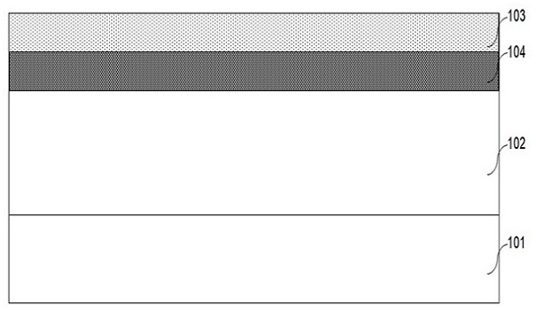
[0041] S1, epitaxial growth on the silicon carbide substrate 101 to form a silicon carbide epitaxial layer 102, specifically as figure 1 shown;

[0042] S2, forming a P-type blocking implantation region 104 on the silicon carbide epitaxial layer 102 by ion implantation of aluminum (Al) or boron (B), with a doping concentration of 5×10 15 cm -3 ~5×10 17 cm -3 , specifically as figure 1 shown;

[0043] S3, forming an N-type source implantation region 103 on the silicon carbide epitaxial layer 102 by implanting nitrogen (N) or phosphorus (P) ions, with a doping concentration of 5×10 16 cm -3 ~1×10 18 cm -3 , specifically as figure 1 shown;

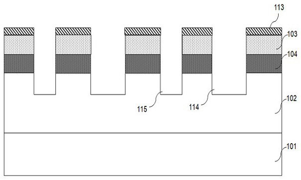
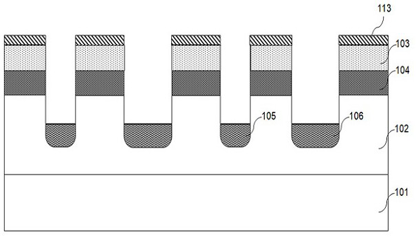
[0044] S4, on the upper surface of the silicon carbide epitaxial layer 102, a patterned mask oxide...

Embodiment 2

[0053] The difference between this embodiment and Embodiment 1 is that the first conductivity type is P, and the second conductivity type is N. Specifically, the preparation method of the high-voltage silicon carbide device is as follows:

[0054] S1, epitaxial growth on the silicon carbide substrate 101 to form a silicon carbide epitaxial layer 102, specifically as figure 1 shown;

[0055] S2, forming an N-type blocking implantation region 104 on the silicon carbide epitaxial layer 102 by implanting nitrogen (N) or phosphorus (P) ions, with a doping concentration of 5×10 15 cm -3 ~5×10 17 cm -3 , specifically as figure 1 shown;

[0056] S3, forming a P-type source implantation region 103 on the silicon carbide epitaxial layer 102 by ion implantation of aluminum (Al) or boron (B), with a doping concentration of 5×10 16 cm -3 ~1×10 18 cm -3 , specifically as figure 1 shown;

[0057] S4, on the upper surface of the silicon carbide epitaxial layer 102, a patterned mask...


PUM


Abstract

The invention discloses a high-voltage-resistant silicon carbide device and a preparation method thereof, the high-voltage-resistant silicon carbide device comprises a silicon carbide substrate, a silicon carbide epitaxial layer arranged on the silicon carbide substrate and a drain metal electrode arranged on the back surface of the silicon carbide substrate, and a blocking injection region and a source injection region are sequentially arranged on the silicon carbide epitaxial layer; a plurality of first grooves and second grooves are etched in the silicon carbide epitaxial layer; a gate protection region is arranged at the bottom of the first groove, an oxide layer grows on the surface of the first groove, a gate polycrystalline silicon electrode is arranged on the oxide layer, and an insulating layer covers the gate polycrystalline silicon electrode; the bottom of the second groove is provided with a voltage-withstanding injection region, and the second groove is provided with a polycrystalline silicon filler. And the source electrode injection region and the insulating layer are covered with a source electrode metal electrode, so that the problems of low reverse voltage and complex process in the prior art are solved.

Description

technical field [0001] The invention relates to the technical field of semiconductors, in particular to a high-voltage silicon carbide device and a preparation method thereof. Background technique [0002] As a wide bandgap material, silicon carbide can achieve low conduction loss, and has excellent high temperature resistance and thermal conductivity, which can meet various application requirements. The high critical field characteristics of silicon carbide materials enable silicon carbide power devices to have higher doping concentrations and thinner drift layer thicknesses than conventional silicon devices at the same voltage, thereby achieving lower on-resistance. The low switching loss and high operating frequency of silicon carbide MOSFET are very suitable for the application requirements of power electronics. [0003] However, due to SiO 2 The interface state density at the (gate oxide) / SiC (silicon carbide) interface is high, and SiC MOSFET devices have the problem...

Claims


Application Information

Patent Timeline
Patent Type & Authority Applications(China)
IPC IPC(8): H01L29/78H01L29/423H01L21/336
CPCH01L29/7813H01L29/4236H01L29/66734
Inventor 王中健曹远迎
Owner 成都功成半导体有限公司
Why Eureka
Try Eureka