Laser annealing method for back-illuminated image sensor

An image sensor and laser annealing technology, which is applied in semiconductor devices, electric solid-state devices, radiation control devices, etc., can solve the problems that the back-illuminated silicon detector does not remove the silicon dioxide layer, and the removal of the silicon dioxide layer is troublesome, and achieves Reduced tunneling effect, good annealing effect

Pending Publication Date: 2022-05-13
SHANGHAI HUAHONG GRACE SEMICON MFG CORP
View PDF0 Cites 0 Cited by
  • Summary
  • Abstract
  • Description
  • Claims
  • Application Information

AI Technical Summary

Problems solved by technology

[0006] The back-illuminated silicon detector does not have a tool to remove the silicon diox

Method used


Image

  • Laser annealing method for back-illuminated image sensor
  • Laser annealing method for back-illuminated image sensor
  • Laser annealing method for back-illuminated image sensor

Examples


Embodiment Construction

[0041] Embodiments of the present invention are described below through specific examples, and those skilled in the art can easily understand other advantages and effects of the present invention from the content disclosed in this specification. The present invention can also be implemented or applied through other different specific implementation modes, and various modifications or changes can be made to the details in this specification based on different viewpoints and applications without departing from the spirit of the present invention.

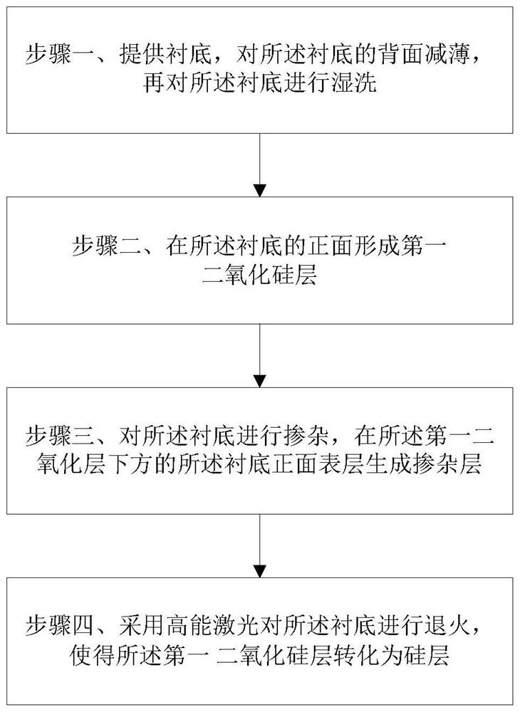
[0042] see figure 1 , the present invention provides a laser annealing method for a back-illuminated image sensor comprising:

[0043] Step 1, provide such as Figure 4 As shown in the substrate 10, the back side of the substrate 10 can be thinned afterwards, and the wafer substrate 10 can be thinned by thinning or grinding to improve the heat dissipation effect of the chip, and at the same time, thinning to a certain thickness is b...


PUM

PropertyMeasurementUnit
Resistivityaaaaaaaaaa
Thicknessaaaaaaaaaa
Thicknessaaaaaaaaaa

Abstract

The invention provides a laser annealing method for a back-illuminated image sensor, which comprises the following steps of: providing a substrate, thinning the back surface of the substrate, and carrying out wet washing on the substrate; forming a first silicon dioxide layer on the front surface of the substrate; doping the substrate, and generating a doped layer at the top end of the substrate; and annealing the substrate by adopting high-energy laser, so that the first silicon dioxide layer is converted into a silicon layer. The silicon dioxide layer is deposited before the substrate is subjected to laser annealing, so that the tunnel effect in the arsenic ion injection process is reduced; the silicon is protected in the laser annealing process, and the local area of the substrate is prevented from being fused at the high temperature generated by laser annealing; the silicon dioxide has a laser anti-reflection effect, so that the annealing effect is better; silicon dioxide will react with carbon and be converted to pure silicon in enhanced laser annealing without wet protection of the front surface.

Description

technical field [0001] The invention relates to the technical field of semiconductors, in particular to a laser annealing method for a back-illuminated image sensor. Background technique [0002] X-ray silicon detector products are mainly divided into two categories: amorphous flat-panel X-ray detectors, and high-end silicon-based X-ray detectors. At present, the domestic technology of amorphous flat-panel X-ray detector is relatively mature, and it has certain international market competitiveness, and its manufacturing process is not compatible with FAB process. Silicon-based X-ray detectors have been developed for two generations. The first-generation product is a front-illuminated process, which is compatible with the FAB process and does not require the backside process of a silicon wafer. The process complexity is relatively low. The second-generation product is a back-illuminated process. Based on the first-generation process, the back-side process of silicon wafers i...

Claims


Application Information

Patent Timeline
IPC IPC(8): H01L27/146
CPCH01L27/14685H01L27/14687H01L27/14698H01L27/1464
Inventor 宗立超王星杰顾培楼
Owner SHANGHAI HUAHONG GRACE SEMICON MFG CORP
Why Eureka
Try Eureka