Method for manufacturing n-metal-oxide-semiconductor (NMOS) transistor

A manufacturing method and transistor technology, applied in semiconductor/solid-state device manufacturing, semiconductor devices, electrical components, etc., can solve the problems of poor performance of semiconductor devices, difficulty in ion implantation depth and concentration, and failure of NMOS transistor resistance and junction depth to meet requirements and other problems, to achieve the effects of reducing the resistance of the source and drain regions, suppressing diffusion and channel effects, and suppressing instantaneously enhanced diffusion and tunneling effects

Active Publication Date: 2013-01-02
SEMICON MFG INT (SHANGHAI) CORP +1
View PDF1 Cites 0 Cited by
  • Summary
  • Abstract
  • Description
  • Claims
  • Application Information

AI Technical Summary

Problems solved by technology

[0006] However, as the size of the device decreases, the depth and concentration of ion implantation become more and more difficult to control, so that the resistance and junction depth of the source and drain regions of the NMOS transistor obtained by the above-mentioned traditional method cannot meet the requirements, thus making The performance of semiconductor devices deteriorates

Method used


Image

  • Method for manufacturing n-metal-oxide-semiconductor (NMOS) transistor
  • Method for manufacturing n-metal-oxide-semiconductor (NMOS) transistor
  • Method for manufacturing n-metal-oxide-semiconductor (NMOS) transistor

Examples


Embodiment 1

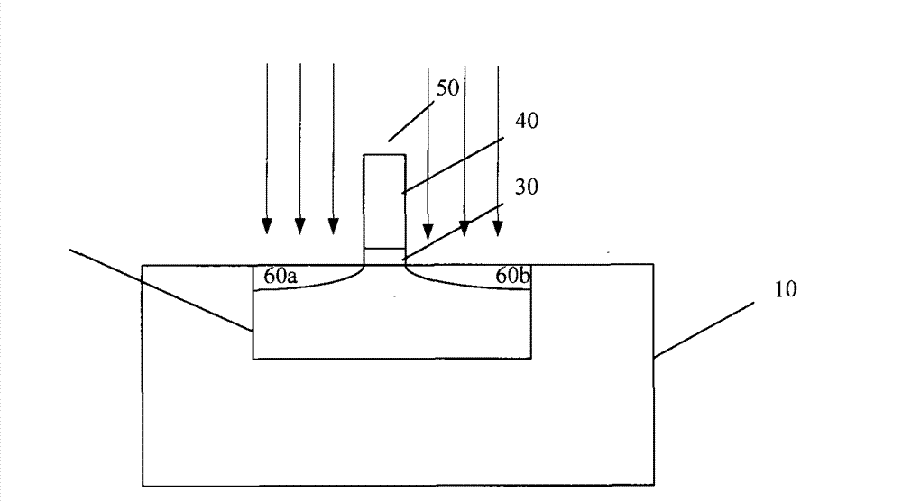
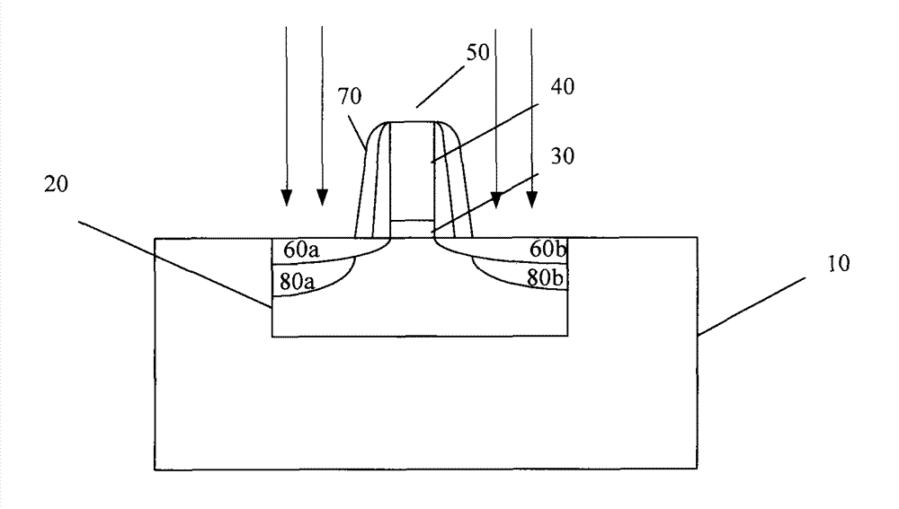
[0057] Figure 4 It is a flow chart of an embodiment of the manufacturing method of the NMOS transistor of the present invention. Figure 5 to Figure 7 It is a schematic diagram of an embodiment of the manufacturing method of the NMOS transistor of the present invention. Combine below Figure 5 to Figure 7 The semiconductor device manufacturing method of the invention is described in detail, the semiconductor device manufacturing method of the present invention includes steps:

[0058] S20: providing a semiconductor substrate having a gate structure on the semiconductor substrate.

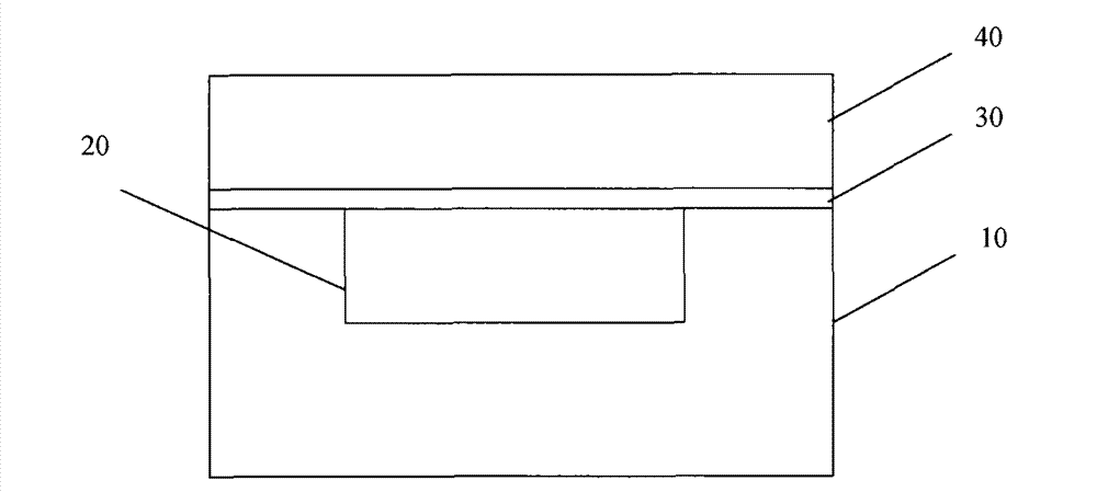
[0059] refer to Figure 5 Specifically, the semiconductor substrate 100 may be silicon or silicon germanium (SiGe) with a single crystal, polycrystalline or amorphous structure, or silicon-on-insulator (SOI), or may also include other materials, such as indium antimonide , lead telluride, indium arsenide, indium phosphide, gallium arsenide, or gallium antimonide. Although several examples of m...


PUM


Abstract

The invention discloses a method for preparing an n-metal-oxide-semiconductor (NMOS) transistor, comprising the following steps: doping antimony ions and carbon ions in a provided semiconductor substrate with a grid structure at the two sides of the grid structure; doping n-type ions in the semiconductor substrate at the two sides of the grid structure to form a source light dope region and a drain light dope region; forming lateral wall spacers at the two sides of the grid structure; and doping n-type ions in the semiconductor substrate at the two sides of the grid structure with the lateralwall spacers to form a source heavy dope region and a drain heavy dope region, thus improving the performance of a semiconductor device.

Description

technical field [0001] The invention relates to the technical field of semiconductor manufacturing, in particular to a manufacturing method of an NMOS transistor. Background technique [0002] With the rapid development of semiconductor manufacturing technology, in order to achieve faster computing speed, larger data storage capacity and more functions of semiconductor devices, semiconductor wafers are developing towards high integration, and the gate feature size of MOS devices has entered deep In the sub-micron stage, the conductive channel under the gate becomes thinner and shorter than before, so the requirements for the process are getting higher and higher. [0003] In conventional semiconductor manufacturing techniques, NMOS transistors are formed, Figure 1 to Figure 3 For a schematic diagram of forming an NMOS transistor using conventional methods, refer to Figure 1 to Figure 3 First, a semiconductor substrate 10 is provided, and a p-well 20 is formed in the semico...

Claims


Application Information

Patent Timeline
Patent Type & Authority Patents(China)
IPC IPC(8): H01L21/336H01L21/265H01L29/38H01L21/316
Inventor 赵猛
Owner SEMICON MFG INT (SHANGHAI) CORP
Why Eureka
Try Eureka