Multi-pulse-width composite printed circuit board laser processing device

A printed circuit board and laser processing technology, which is applied in the direction of manufacturing tools, metal processing equipment, laser welding equipment, etc., can solve the problems of high equipment cost and low drilling efficiency, improve processing quality, improve drilling efficiency, The effect of ensuring power stability

Active Publication Date: 2022-07-01
杭州凌像科技有限公司
View PDF23 Cites 0 Cited by
  • Summary
  • Abstract
  • Description
  • Claims
  • Application Information

AI Technical Summary

Problems solved by technology

[0007] The present invention aims to overcome the problems of low drilling efficiency and high equipment cost in the existing laser drilling technology in the prior art, and provides a multi-pulse width compound laser drilling machine that can improve processing speed, improve processing quality and save equipment cost. printed circuit board laser processing device

Method used


Image

  • Multi-pulse-width composite printed circuit board laser processing device
  • Multi-pulse-width composite printed circuit board laser processing device
  • Multi-pulse-width composite printed circuit board laser processing device

Examples


Embodiment 1

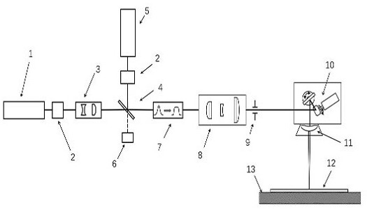
[0036] like Figure 1 to Figure 3 The shown multi-pulse width composite printed circuit board laser processing device includes nanosecond pulse laser 1, ultrafast laser 5, manual variable magnification mirror group 3, beam combiner 4, beam shaper 7, automatic variable magnification mirror Group 8, aperture regulator 9, galvanometer 10, field mirror 11 and translation stage 13; optical isolators 2 are provided between the nanosecond pulse laser and the manual variable magnification mirror group and between the ultrafast laser and the beam combiner ; The extension direction of the ultrafast laser light path is provided with a light absorber 6 for absorbing the ultrafast light pulses leaked from the beam combiner and the reflected nanosecond light pulses.

[0037] like figure 1 As shown, the optical path is divided into two paths before the beam combiner, figure 1 The middle-level one is provided with nanosecond pulse laser, optical isolator, and manual variable magnification mir...

Embodiment 2

[0063] like Figure 4 As shown, this embodiment also provides a double-table laser processing device. In order to improve production efficiency, common PCB laser drilling machines usually adopt a double-station linkage design, which requires two optical paths on the two stations of the translation table. processing. In terms of cost, it is more cost-effective to split a single ultrafast laser into two channels. At the same time, since the peak power of the ultrafast laser itself is high enough, the peak power of each channel after splitting into two channels is also sufficient to destroy the surface of the material; therefore In this embodiment, the ultrafast laser is divided into two paths by a beam splitter 14 after passing through the optical isolator and the manual variable magnification lens group. The beam splitter can use a polarizing beam splitting prism, and the beam splitting energy ratio can be adjusted by finely adjusting the angle of the beam splitting prism. How...


PUM

PropertyMeasurementUnit
poweraaaaaaaaaa

Abstract

The invention belongs to the technical field of laser processing, and particularly relates to a multi-pulse-width composite printed circuit board laser processing device. Comprising a nanosecond pulse laser, an ultrafast laser, a beam combiner, a beam shaper, an automatic zoom lens group, an aperture regulator, a galvanometer and a field lens, the nanosecond pulse laser emits light beams to the beam combiner; the ultrafast laser emits light beams to the beam combiner; the beam combiner is used for converting the light beam emitted by the nanosecond pulse laser and the light beam emitted by the ultrafast laser into a combined light beam sharing the same optical axis in space; the light beam shaping device is used for converting the combined light beam into a flattop Gaussian light beam; the automatic zoom lens group is used for automatically changing the diameter of the flattop Gaussian beam; the flattop Gaussian beam passes through the aperture regulator, and the aperture regulator is used for intercepting stray light; the galvanometer is used for emitting flat-topped Gaussian beams which are deflected at a high speed to the field lens; and the field lens emits the focused flattop Gaussian beam to the printed circuit board.

Description

technical field [0001] The invention belongs to the technical field of laser processing, in particular to a multi-pulse width composite printed circuit board laser processing device. Background technique [0002] Printed circuit boards (PCBs) are the main components used to carry and connect electronic components in various electronic devices. With the rapid development of electronic products represented by smartphones, smart wearable devices, computers, etc., the interconnection density of PCBs There are higher and higher requirements. A high-density PCB is usually a multi-layer structure. The wiring between different layers is mainly connected by vias. The processing of vias mainly includes mechanical drilling and laser drilling. Mechanical drilling is to drill the circuit board with a micro drill bit rotating at high speed. Due to the limitation of the drill bit diameter, when the diameter of the via hole is less than 200 microns, the drill bit is too thin, resulting in ...

Claims


Application Information

Patent Timeline
Patent Type & Authority Applications(China)
IPC IPC(8): B23K26/382B23K26/70
CPCB23K26/382B23K26/702
Inventor 李华兵孙东明林汇文杨恺伦
Owner 杭州凌像科技有限公司
Why Eureka
Try Eureka