Angle sensor and manufacturing process thereof
An angle sensor and manufacturing process technology, applied in the field of magnetic field sensors, can solve problems such as low precision and sensitivity, difficult angle measurement, and large volume, and achieve the effects of simple operation, easy mass production, and miniaturization
- Summary
- Abstract
- Description
- Claims
- Application Information
AI Technical Summary
Problems solved by technology
Method used
Image
Examples
Embodiment approach
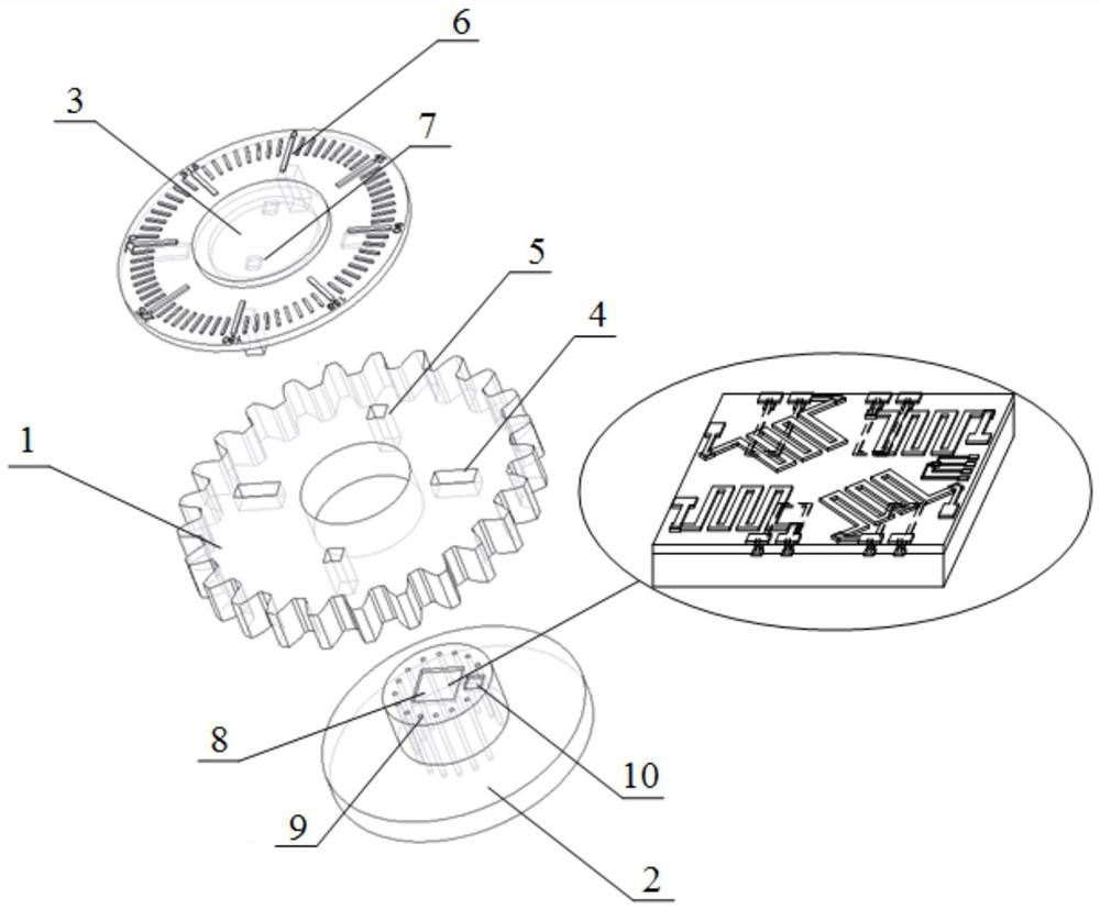
[0080] According to a preferred embodiment of the present invention, the rotor 1 is a disc structure, and a circular through slot is opened in the center to be nested and connected to the stator base,
[0081] The edge of the rotor 1 is a tooth-like structure.
[0082] In a further preferred embodiment, the rotor 1 is provided with small rotor magnets 4 , there are two small rotor magnets, and the two are distributed along the diameter of the rotor 1 and symmetrically distributed with respect to the center of the rotor 1 .
[0083] Wherein, the small rotor magnets are arranged in the disc plate surface of the rotor 1 .
[0084] Preferably, the two small rotor magnets are arranged in the same direction of magnetic sensitivity.
[0085] In the present invention, the two small rotor magnets generate a uniform magnetic field in the horizontal direction, which is applied to the first magnetic sensitive unit.
[0086] More preferably, the rotor is made of a wear-resistant resin ma...
Embodiment 1
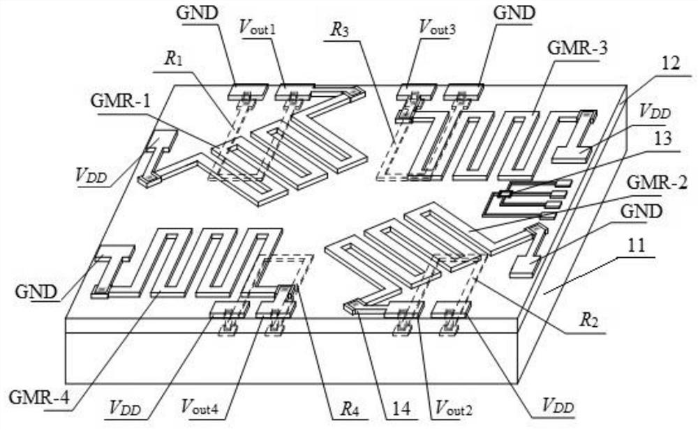
[0187] (1) Make the magnetic sensitive unit of the angle sensor according to the following steps:
[0188] Step 1, zero-shot lithography, dry etching the silicon wafer registration mark.
[0189] Step 2, cleaning the silicon wafer, performing the first oxidation by thermal oxidation, and growing a thin oxygen layer on one side of the upper surface of the silicon wafer with a thickness of 30 nm.
[0190] Wherein, the silicon wafer is a crystal orientation p-type single crystal silicon wafer, the thickness of a 4-inch wafer is 500 μm, and the resistivity is 0.1 Ω·cm.
[0191] The cleaning of the silicon wafer adopts the RCA standard cleaning method.
[0192] Step 3, the first photolithography, the ion implantation window is formed, and phosphorus ions are implanted on the upper surface of the silicon wafer to form the magnetic sensitive area of the Hall element and four diffusion resistors.
[0193] Among them, the magnetic sensitive area and the four diffusion resistances ...
experiment example 1
[0215] Using a magnetic field generator (recommended model of Beijing Cuihai Jiacheng Magnetoelectric Technology Co., Ltd.: CH Hall-300, which can generate a magnetic field of 1Gs ~ 1T), a stepping motor drive controller (CH-400B), a program-controlled power current source (CH-HallModel F2030), full digital high-resolution Tesla meter (CH-1600), programmable linear DC power supply (RIGOLDP832A) from Suzhou Puyuan Precision Technology Co., Ltd. and data collector (Agilent 34410A) and other instruments to test the magnetic properties of the magnetic sensitive unit of the angle sensor prepared in Example 1.
[0216] Specifically, under the condition of room temperature (300K), the magnetic sensitive unit of the angle sensor is placed in the magnetic field environment of the test system, and the power supply voltage V DD = 5.0V, the rotation angle range is 0°~360°, and the rotation step is 1° (adjust the magnetic field size to 5.0mT, 10.0mT, 15.0mT respectively), and test the char...
PUM
| Property | Measurement | Unit |
|---|---|---|
| Thickness | aaaaa | aaaaa |
| Resistivity | aaaaa | aaaaa |
| Thickness | aaaaa | aaaaa |
Abstract
Description
Claims
Application Information


