Method for judging sub-crystal domain and crystal lattice direction of rhenium compound film based on optical method
A compound and lattice orientation technology, which is applied in the direction of material analysis, scientific instruments, and instruments through optical means, can solve the problems of high equipment requirements, decreased electrical mobility, and obstacles to large-scale device applications, and meet the requirements of equipment conditions The effect of low cost and simple operation process
- Summary
- Abstract
- Description
- Claims
- Application Information
AI Technical Summary
Problems solved by technology
Method used
Image
Examples
Embodiment 1
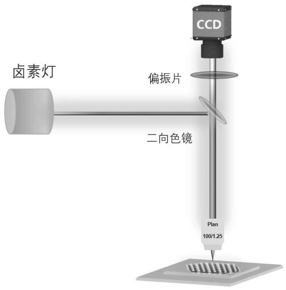
[0035] In this example, an optical microscope is used to determine the sub-domains and grain boundaries of the rhenium disulfide thin film, and the optical path diagram of the experimental device used is as follows figure 1shown.
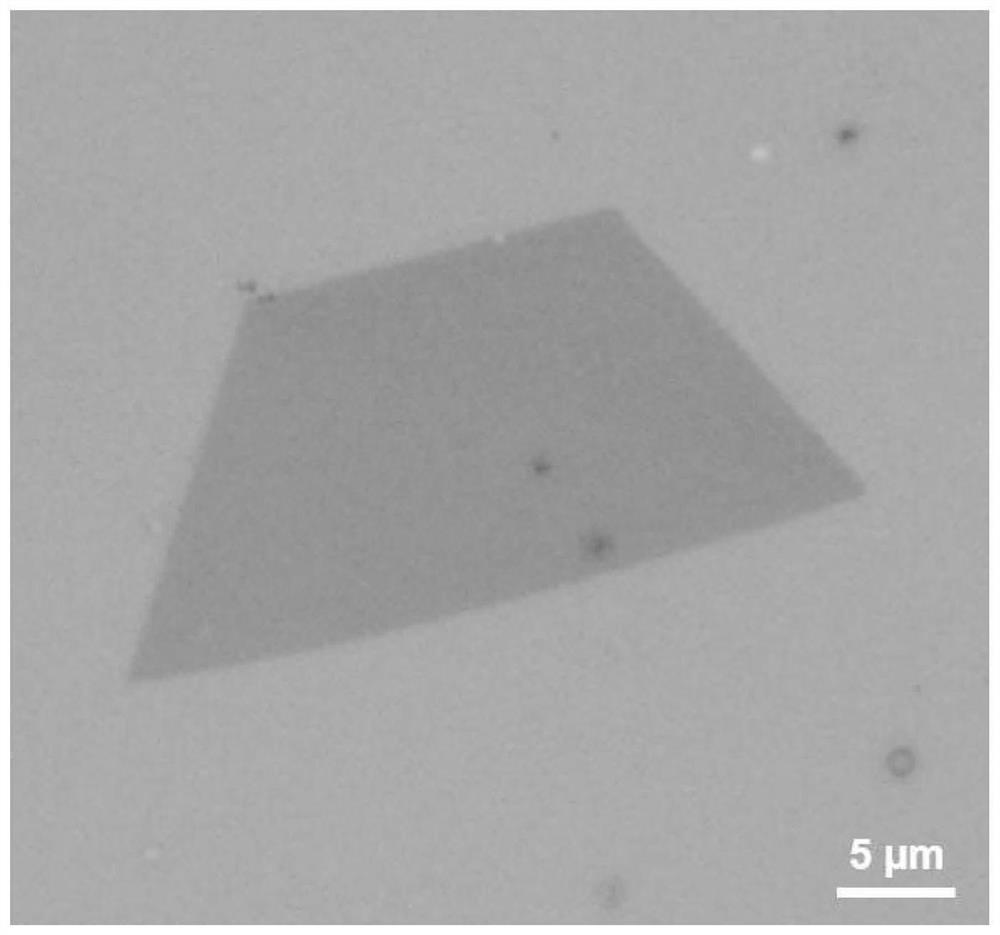
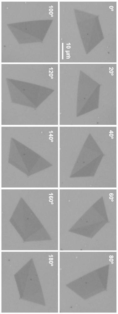
[0036] A freely insertable external polarizer is placed in the collecting light path of the optical microscope, and the polarizing direction of the polarizer is the x direction, which will be transferred to 300nm thick SiO 2 / The rhenium disulfide sample on the Si substrate is placed on the stage of the optical microscope, the sample stage is rotated every 20°, and the photo is taken. The obtained sample photos under different rotation angles are as follows: image 3 It can be seen that with the change of the rotation angle of the sample, different regions show obvious contrast differences. According to the contrast differences, we can divide the trapezoidal rhenium disulfide sample into three regions, such as Figure 4 As shown, they are represen...
Embodiment 2
[0039] The rhenium disulfide used in this example is few-layer ReS grown at 800°C 2 .
[0040] A freely insertable external polarizer is placed in the collecting light path of the optical microscope, and the polarizing direction of the polarizer is the x direction, which will be transferred to 300nm thick SiO 2 The rhenium disulfide sample on the / Si substrate was placed on the stage of the optical microscope, the sample stage was rotated every 20°, and photographs were taken.
[0041] RGB contrast extraction was performed on the photographed photos to obtain the lattice orientation of each subdomain.
[0042] Figure 8 Few-layer ReS grown at 800°C 2 Photographs under a polarized light microscope and periodograms of B channel changes in the corresponding regions. Figure 8 (a) is an optical micrograph at a rotation of 40°, which can be divided into two regions according to the contrast difference, respectively using and represents, and plots the relative contrast of th...
Embodiment 3
[0044] The rhenium disulfide used in this example is a thick layer of ReS grown at 900°C 2 .
[0045] A freely insertable external polarizer is placed in the collecting light path of the optical microscope, and the polarizing direction of the polarizer is the x direction, which will be transferred to 300nm thick SiO 2 The rhenium disulfide sample on the / Si substrate was placed on the stage of the optical microscope, the sample stage was rotated every 20°, and photographs were taken.
[0046] RGB contrast extraction was performed on the photographed photos to obtain the lattice orientation of each subdomain.
[0047] Figure 9 Few-layer ReS grown at 900°C 2 Photographs under a polarized light microscope and periodograms of B channel changes in the corresponding regions. Figure 9 (a) is an optical micrograph at a rotation of 40°, which can be divided into two regions according to the contrast difference, respectively using and represents, and plots the relative contras...
PUM
| Property | Measurement | Unit |
|---|---|---|
| Length | aaaaa | aaaaa |
Abstract
Description
Claims
Application Information


