Silicon carbide super-structure surface for high-gain ultraviolet photoelectric detector and preparation method of silicon carbide super-structure surface
A metasurface, electrical detector technology, applied in circuits, electrical components, nano-optics, etc., can solve the problem of limited improvement of grating structure, and achieve the effect of improving the intensity of photocurrent
- Summary
- Abstract
- Description
- Claims
- Application Information
AI Technical Summary
Problems solved by technology
Method used
Image


Examples
Embodiment 1
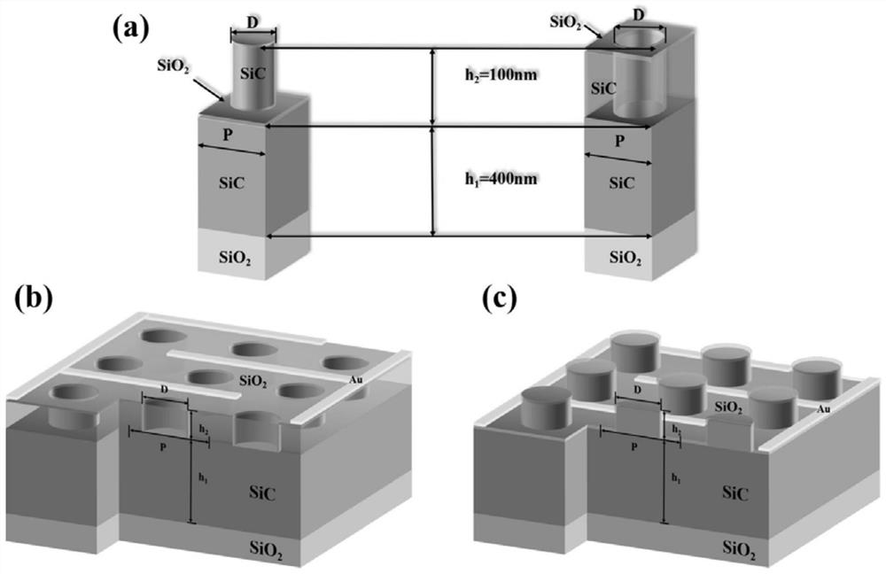
[0036] like figure 1 As shown in (a)-1(c), a silicon carbide metasurface for high-gain ultraviolet photodetectors includes:
[0037] insulating substrate;
[0038] The silicon carbide layer is arranged on the surface of the insulating substrate;
[0039] The silicon carbide metasurface is arranged on the surface of the silicon carbide layer;
[0040] Wherein, the superstructured surface of silicon carbide includes nano-columns or nano-pore micro-structures, the nano-columns or nano-pore micro-structures have the same spacing, and are periodically arranged on the surface of the silicon carbide layer according to the tetragonal lattice, and the material of the micro-structure is carbide. silicon;
[0041] The anti-reflection coating layer is arranged on the surface layer of the superstructured silicon carbide surface, and the material of the anti-reflection coating layer is silicon dioxide;
[0042] Electrodes are arranged on the surface of the anti-reflection coating.
[0...
Embodiment 2
[0052] The present embodiment provides a method for preparing a silicon carbide metasurface for a high-gain ultraviolet photodetector, comprising the following steps:
[0053] S1. Use highly symmetrical nano-pillars or nano-hole microstructures to design the silicon carbide metasurface, so as to reduce the sensitivity of the silicon carbide metasurface microstructure to the polarization state of incident light;
[0054] S2. Select the microstructure of subwavelength size to modify the silicon carbide layer, and optimize the size of the microstructure to achieve the effect of broadband absorption enhancement;
[0055]S3. On the basis of the silicon carbide metasurface, an anti-reflection coating is added to further improve the broadband absorption effect of the silicon carbide metasurface in the ultraviolet band.
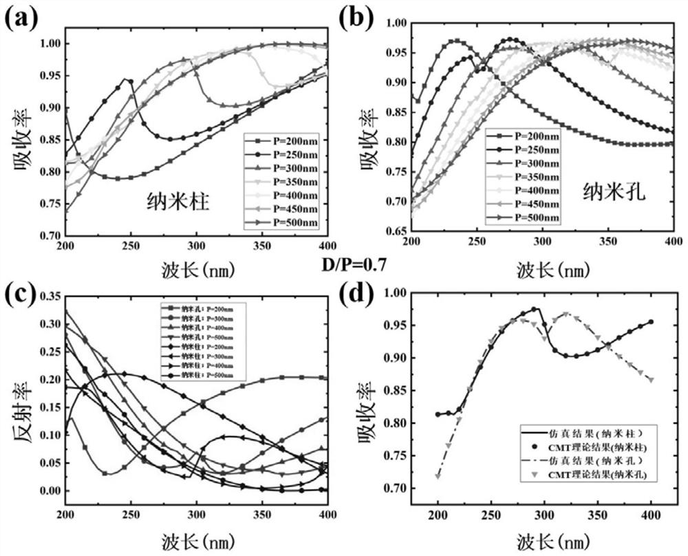
[0056] The design process is specific, first considering the design of the SiC metasurface without the capping layer. The SiC metasurface adopts the microstructure ...
PUM
| Property | Measurement | Unit |
|---|---|---|
| diameter | aaaaa | aaaaa |
| thickness | aaaaa | aaaaa |
| thickness | aaaaa | aaaaa |
Abstract
Description
Claims
Application Information