Prepn of nitride-oxide film
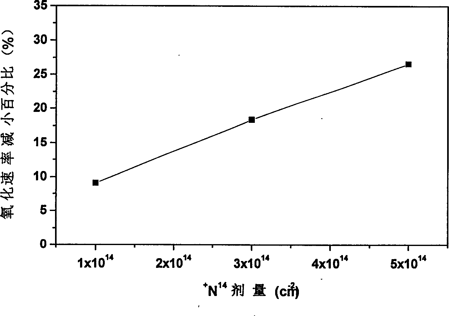
An oxide film and pre-oxidation technology, which is applied in semiconductor/solid-state device manufacturing, electrical components, circuits, etc., can solve the problem that the nitrided oxide gate dielectric cannot be applied to devices and circuits, etc., to reduce the direct tunneling leakage current and improve the density Sexuality, the effect of reducing the oxidation rate
- Summary
- Abstract
- Description
- Claims
- Application Information
AI Technical Summary
Problems solved by technology
Method used
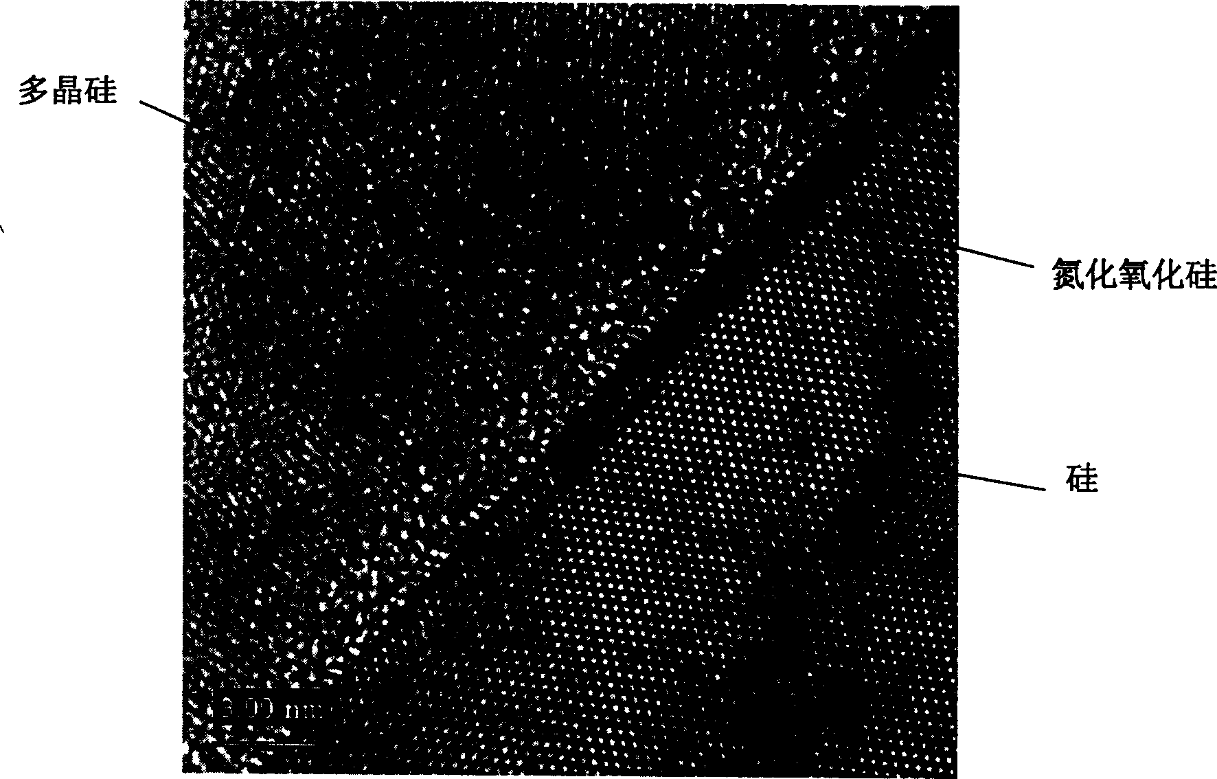
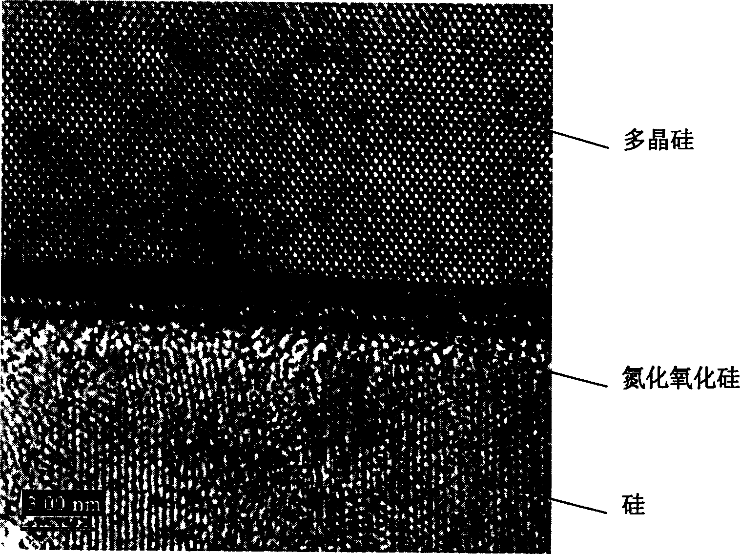
Image

Examples
Embodiment
[0027] The formula of the cleaning liquid that the present invention adopts is:
[0028] 3 # Liquid formula: H 2 SO 4 :H 2 o 2 =5:1 (volume ratio)
[0029] 1 # Liquid formula: NH 4 OH:H 2 o 2 :H 2 O=0.8:1:5 (volume ratio)
[0030] HF / IPA formula: HF:IPA:H 2 O=0.5%:0.02%:1
[0031] 1. Wafer cleaning: 3 # Liquid degumming for 10 minutes, 3 # Liquid cleaning 10 minutes, 1 # liquid wash for 5 minutes, H 2 O / HF (20 / 1) drift for 15 seconds.
[0032] 2. Pre-oxidation: thick 150 Å, 850 ℃, dry O 2 , 170 points+N 2 , annealed for 30 minutes.
[0033] 3. Chemical vapor deposition (LPCVD) Si 3 N 4 : Thickness 1300 Å, 780°C.
[0034] 4. Cleaning: 3 # solution for 10 minutes, 1 # Liquid 5 minutes, H 2 O / HF (1 / 20), drift for 15 seconds.
[0035] 5. Si 3 N 4 Annealing: 800°C, N 2 , annealed for 30 minutes.
[0036] 6. Photolithographic active area: 9912 glue, 1.2 μm.
[0037] 7. Reactive ion etching Si 3 N 4 : SiO is left in the active area 2 80 Å, power 150...
PUM
 Abstract
Description
Claims
Application Information
 - R&D
- Intellectual Property
- Life Sciences
- Materials
- Tech Scout
- Unparalleled Data Quality
- Higher Quality Content
- 60% Fewer Hallucinations
Browse by: Latest US Patents, China's latest patents, Technical Efficacy Thesaurus, Application Domain, Technology Topic, Popular Technical Reports.
© 2025 PatSnap. All rights reserved.Legal|Privacy policy|Modern Slavery Act Transparency Statement|Sitemap|About US| Contact US: help@patsnap.com