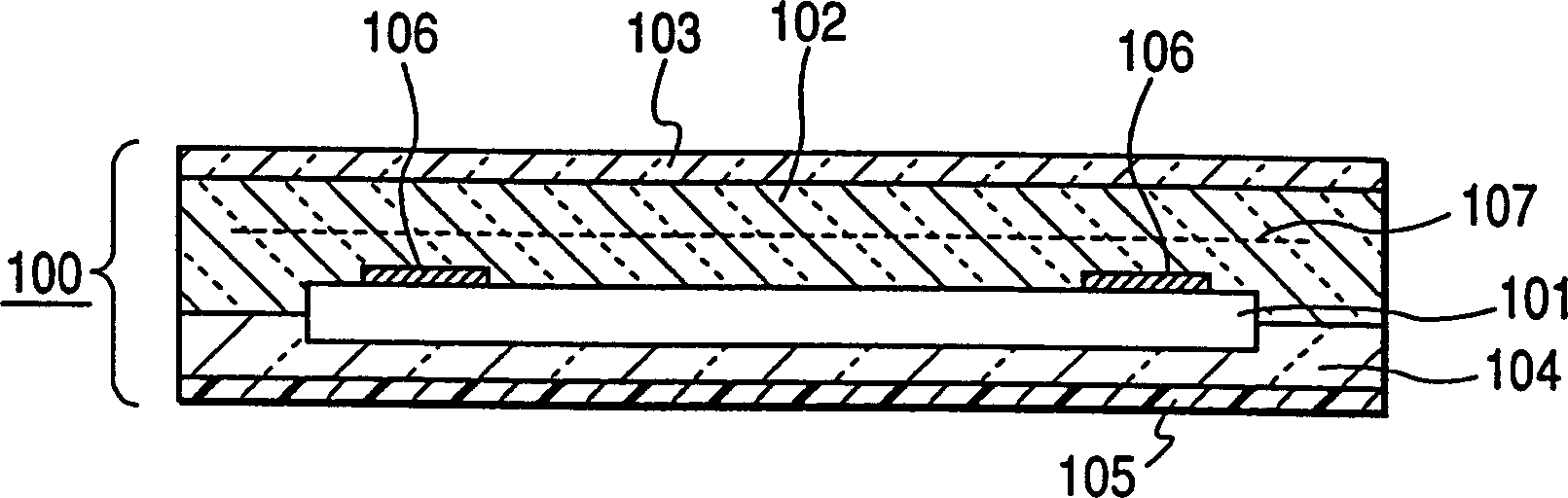
Encapsulant resin member for semiconductor, and semiconductor element
A photovoltaic and sealing resin technology, which is applied in photovoltaic power generation, electrical components, semiconductor/solid-state device components, etc., can solve the problems of appearance degradation and lower yield of solar cell components, and achieve the effect of preventing degradation
- Summary
- Abstract
- Description
- Claims
- Application Information
AI Technical Summary
Problems solved by technology
Method used
Image

Examples
example 1
[0059] (Preparation of photovoltaic element part)
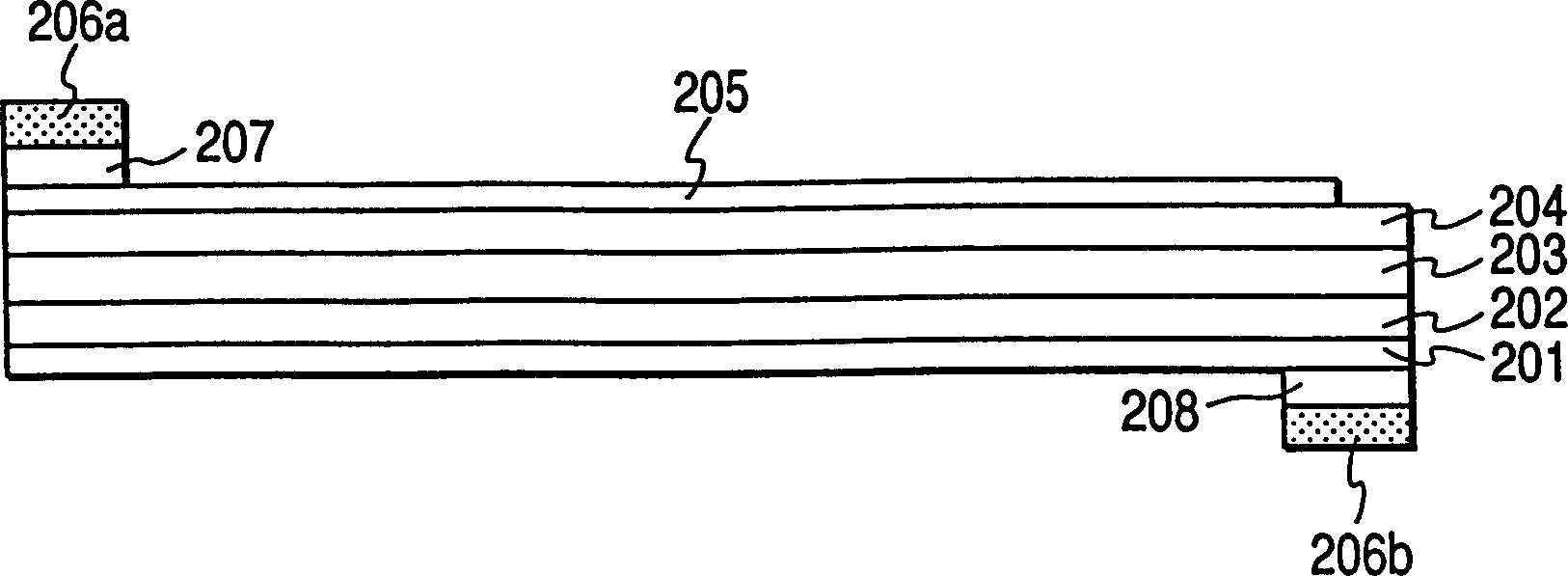
[0060] The amorphous silicon (a-Si) solar cell part (photovoltaic element part) fabricated below is shown in Figure 2A and 2B in the structure. Specifically, an Al layer (5000 Å thick) and a ZnO layer (5000 Å thick) were sequentially formed on a clean stainless steel substrate 201 as the back reflection layer 202 by sputtering. Then, by plasma CVD method, from SiH 4 、PH 3 and H 2 The mixed gas forms the n-type a-Si layer, made of SiH 4 and H 2 The mixed gas forms the i-type a-Si layer, composed of SiH 4 , BF 3 and H 2 The mixed gas forms a p-type microcrystalline μc-Si layer, thereby forming a p-type microcrystalline μc-Si layer, thereby forming an n-layer 150 Å thick / i layer 4000 Å thick / p layer 100 Å thick / n layer 100 Å thick / i layer 800 Å thick / p layer 100 Å The tandem type a-Si photoelectric conversion semiconductor layer 203 is formed in a thick layer structure. Then by resistance heating at O 2 Evaporate in...
example 2
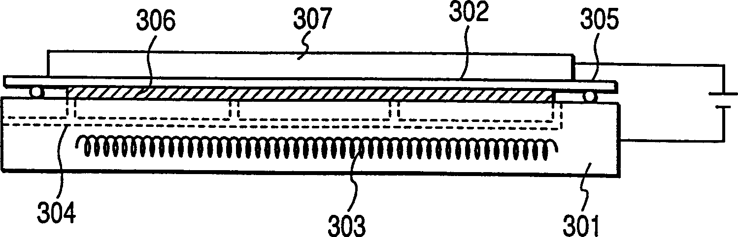
[0067] The same method as in Example 1 was used except that an electric field of 3 KV / mm was applied at the stage of preparing an EVA sheet (460 μm thick) as the front surface sealing resin, and no electric field was applied between the electrode 307 and the sheet 301 during the lamination operation Lamination operations were carried out and the assemblies thus obtained were evaluated.
example 3
[0069] A first EVA resin plate (230 μm thick) containing 1.0 parts by weight of a silane coupling agent relative to 100 parts by weight of EVA and not containing an ultraviolet absorber was placed on the photoelectric conversion element portion, containing 0.3 parts by weight of ultraviolet rays relative to 100 parts by weight of EVA Absorbent and a second EVA resin sheet (230 μm thick) without silane coupling agent are placed on the first sheet, the two resin sheets are bonded to form the front surface sealing resin, and the electrode 307 and the sheet 301 are bonded during the lamination operation. The lamination operation was performed in the same manner as in Example 1 except that no electric field was applied between them, and the assemblies thus obtained were evaluated.
PUM
 Abstract
Description
Claims
Application Information
 - R&D
- Intellectual Property
- Life Sciences
- Materials
- Tech Scout
- Unparalleled Data Quality
- Higher Quality Content
- 60% Fewer Hallucinations
Browse by: Latest US Patents, China's latest patents, Technical Efficacy Thesaurus, Application Domain, Technology Topic, Popular Technical Reports.
© 2025 PatSnap. All rights reserved.Legal|Privacy policy|Modern Slavery Act Transparency Statement|Sitemap|About US| Contact US: help@patsnap.com